Columbia VLSI
Digital VLSI Circuits Design
Design Digital VLSI Circuits
Columbia Integrated Systems Laboratory, Columbia University, 2009
Design an 8-bit microcontroller core, implemented in TSMC CMOS process, Digital VLSI Circuits
Designed an 8-bit microcontroller core to perform essential functions within the clock distribution system.
Score: 95/100
- Project Overview: Completed a professional report under the guidance of Professor Kenneth L. Shepard, focusing on the design and implementation of a controller core.
- Tools and Platform: Utilized industry-standard EDA/CAD tools, including Cadence Composer, Virtuoso, Assura; Synopsys HSPICE, Nanosim; Mentor Calibre on a Linux OS platform. Designs were implemented in TSMC 0.25um process, with clean DRC and LVS and final GDSII submission.
![]()
![]() This project employed industry-standard EDA/CAD tools from Cadence, Synopsys, and Mentor (acquired
This project employed industry-standard EDA/CAD tools from Cadence, Synopsys, and Mentor (acquired ![]() by Siemens in 2017) on the GNU/Linux OS:
by Siemens in 2017) on the GNU/Linux OS:
-
- Synopsys Nanosim for timing analysis
- Cadence Ultrasim for timing analysis (now)
- Cadence Composer for schematic entry
- Cadence Schematic Editor for schematic entry (now)
- Cadence Virtuoso for layout design
- Synopsys HSPICE for circuit simulation
- Cadence Spectre for circuit simulation (now)
- Mentor Calibre for layout verification
- Cadence Assura for extraction
- Siemens Calibre for extraction (now)
- Chip Functionality: Designed a controller to execute memory read/write operations, data transfers between internal and external buses, and arithmetic operations (add, subtract, multiply). Functional blocks included full adder, shifter, bus driver, decoder, memory, and PLAs.
- Physical Design Considerations: Addressed floorplanning, placement and routing (P&R, PnR), timing closure, congestion mitigation, power optimization, etc., throughout the design flow.
- Floorplan Strategy: Aligned dataflow signals horizontally and control signals vertically. Layer usage included vertical M1, horizontal M2, and M3 for power/ground distribution.
- Timing closure: Resolved setup violations by upsizing repeaters and shortening critical paths or repeater spacing; addressed hold violations with repeater insertion (buffers or inverters). It is important to note that the optimal repeater spacing exists to minimize the delay of interconnect with repeater insertion.
- Congestion Management: Handled localized routing congestion by refining the floorplan and preserving routing margins, avoiding increased die size or metal layers to control manufacturing cost and yield.
- Power Optimization: Applied multi threshold voltage (multi-Vt) design methodology. High-Vt transistors were used to reduce leakage, with low-Vt selectively applied to critical timing path. Final design minimized dynamic, switching, internal, and leakage power by balancing performance and power trade-offs.
- Glitch Prevention: Replaced latches with edge-triggered D flip-flops (DFFs) to prevent glitches from propagating to subsequent stages.
- Verification and Simulation: Verified functionality and timing through HSPICE and Nanosim simulation. Utilized a combination of HSPICE and Nanosim simulations to verify the clock cycle time, to calculate power dissipation. Used Programmer’s Hierarchical Interactive Graphics System (PHIGS) Extension to X (PEX) for parasitic extraction and logic verification, to verify that core and dataflow functional units were functionally correct. Leveraged Espresso to optimize PLA-based controller logic.
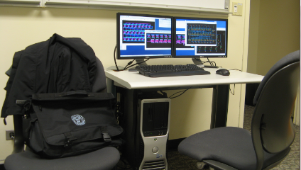 Fig. 1 Research Lab
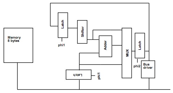 Fig. 2 Datapath of Core Chip
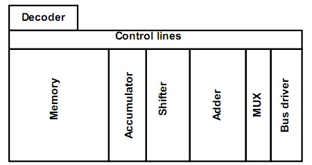
Fig. 3 Floorplan of Core Chip
From the power.log (refer the attachment, please)
Node: Vdd!
Average current: -2.92651e+03uA
RMS current: 2.98727e+03uA
Current peak #1: -2.22710e+04 uA at 6.00000e+02 ns
Current peak #2: -1.96480e+04 uA at 1.80000e+03 ns
Current peak #3: -1.45940e+04 uA at 1.20000e+03 ns
Current peak #4: -5.46200e+03 uA at 1.20121e+03 ns
Current peak #5: -4.77600e+03 uA at 6.00075e+03 ns
Blocks or Modules:
- Full adder 8 bit
- Left shifter and shift by pass 8 bit
- SRAM Read Write Operation
- MUX and Latch
- PLA and Bus Driver
- Micro Controller Core
Return to Projects
The VLSI design project seems simple, but the chip is interesting to me. 😉
Comments
So empty here ... leave a comment!