Cacti++
Cacti++
Github: https://github.com/zp2130/cacti
The research project is a collaborative undertaking between the University of Texas at Arlington (UTA) and Interuniversity Microelectronics Centre (IMEC). A confidentiality agreement has been duly executed by UTA and IMEC. Under copyright and intellectual property protection regulations, the executable file, technology data file, and source code are not available for online distribution. We appreciate your consideration.
[News] UTA aims to build a better microchip – Electrical engineer works to improve on-chip interconnect performance – Written by Jeremy Agor, College of Engineering, Jan. 29, 2021.
https://www.uta.edu/news/news-releases/2021/01/29/pan-microchips, pdf.
[News] UTA aims to build a better microchip – Electronic Business Daily, Feb. 11, 2021. pdf.
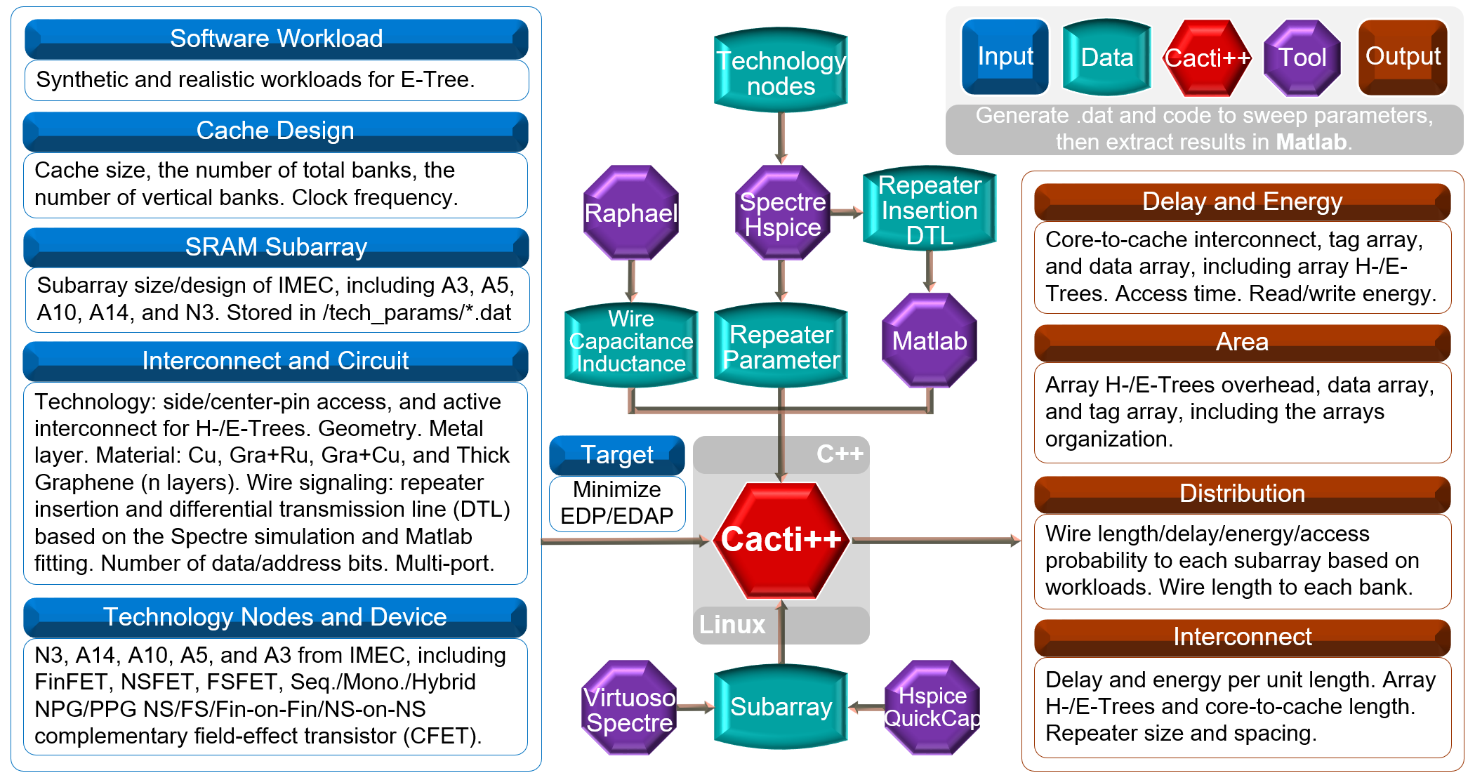
The open-source CACTI simulator, a widely recognized tool, is adopted and modified to optimize the cache memory system. CACTI employs a systematic approach to adjusting SRAM cache memory organization parameters, with the objective of achieving optimal metrics as defined by the users. These metrics may include, for instance, minimum energy-delay product (EDP) or energy-delay-area product (EDAP) for performance-power-area (PPA). To integrate the IMEC-designed subarray, key performance metrics in the original CACTI, such as area, energy, and delay, are incorporated based on true and reliable values extracted from experimental simulations and data in Cadence Virtuoso/Spectre and Synopsys Hspice/QuickCap. The Cacti-based framework, Cacti++, incorporates the overhead associated with the tag array within the cache memory system. The extraction of interconnect and device level parameters is conducted using Cadence Spectre and Synopsys Raphael, with the utilization of state-of-the-art technology nodes from IMEC.
In the Linux operating system, the Cacti++ framework contains an executable file developed by C++, as well as technology parameter data files and code for performing simulations in a large exploration space with high speed and low resource consumption, generated by Matlab. These are automatically generated to systematically sweep input design parameters for the aforementioned executable file and result extraction. The objective of this process is to comprehensively investigate energy-efficient computing systems, spanning from technology node level to system level (a cache memory system), with consideration of both software and hardware.
The Cacti++ framework for co-designing the cache memory system with tag array overhead, interconnect, and technology node in microarchitecture exploration has been developed. The framework incorporates validated experimental subarray designs under a variety of ultra-scaled advanced device technology nodes.
We put forth a proposal and quantify the benefits and constraints of E-Tree design technology with real workload memory allocation, with the aim of improving data average access delay and energy efficiency.
The cache array E-/H-Tree is redesigned by placing repeaters in a strategic manner along the path, with a range of delay overheads compared to optimal delay, in order to obtain the true benefit of the device and trees for the SRAM cache system performance.
The impact of cache design parameters, such as the subarray size/design, the number of vertical banks, and the array E-Tree interconnect level, on cache performance is investigated.
| Platform: | Linux OS |
| Code: | C++; Matlab;Tcl; Slurm; Sbatch. |
| EDA: | Cadence Spectre, Virtuoso; Synopsys Hspice, Raphael, QuickCap. |
Summary of Model Evolution
| Interconnect Device Technology | ASU PTM [6] | IMEC N3 (iN5) [7–9, 14, 16] | IMEC A14 (iN3) [12, 13, 15, 17, *] | 1 | |||||
| Repeater Insertion | Repeater vs DTL | 2 | |||||||
| Subarray | PTM-based bitline for materials | High-level Subarray Model | IMEC-designed A3–14 | 3 | |||||
| Organization | Memory Cells/ Subarray/Mat/Bank/Array | Subarray/Mat/Bank/Array | 4 | ||||||
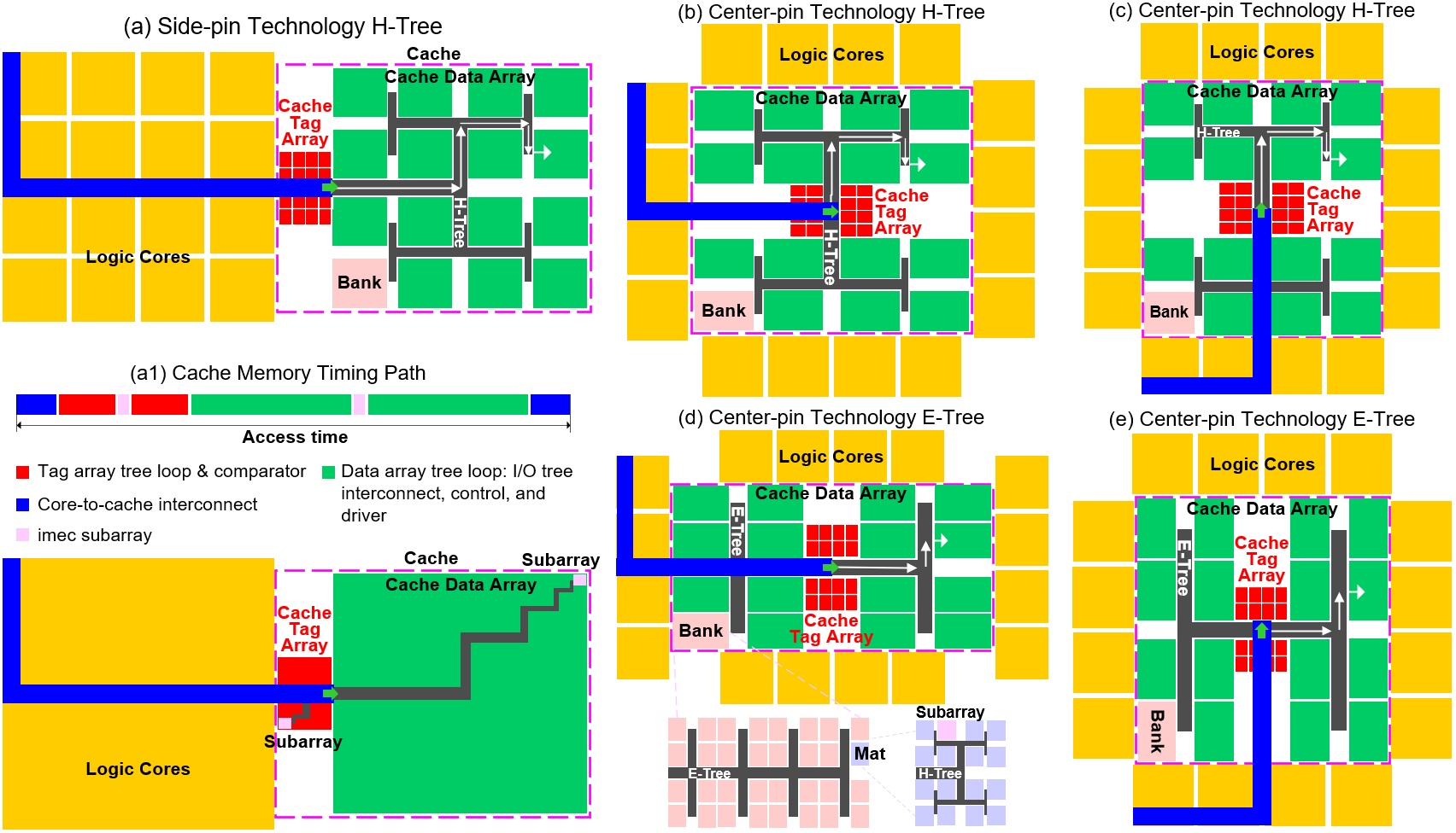
| Pin Type | Original Side Pin | Side Pin or Center Pin or Nonconventional | 5 | ||||||
| Tree Type | Original H-Tree | H-Tree or E-Tree | 6 | ||||||
| Cache/Array | Original arrays, no logic cores. | Data array, Alogic=Asum_subarray | Cache with tag array overhead, Alogic=Acache | 7 | |||||
| Interconnect Delay/Energy | Original equation-based 30% delay overhead for Tpu/Epu | Closed-form Model, Spectre simulation & Matlab fitting | 8 | ||||||
| Interconnect RC/RLC | Original assumptions | Cpu is extracted by Synopsys Raphael | DTL adopts RLC | 9 | |||||
| 1 | 2 | 3 | 4 | 5 | 6 | 7 | 8 | 9 | 10 |
| Metrics | →Model Development Timeline→ |
||||||||
A single simulation:
$./cacti -infile cache.cfg > cache.cfg.log
To sweep the design parameters:
| sbatch_slurm_*_xx_folders_imec_*_hetree.sh
#SBATCH –nodes=1 –cpus-per-task=2 #SBATCH –array=1-xx #SBATCH -p defq cd /path/cacti_$SLURM_ARRAY_TASK_ID source perform_generateCACTI_imec.tcl |
It is recommended that the sbatch, slurm, and tcl be employed for the sweeping of the design parameters. The sbatch, slurm, and tcl code are automatically generated by Matlab. |
| /path/cacti_xx/perform_generateCACTI_imec.tcl
$../cacti -infile cache.cfg -tech_path ../cacti_xx/ > *.log |
A single executable file is located at the root of the simulation folder, which contains xx sub-folders. The file path for the technology is located within each subfolder. |
cache.cfg contains the following parameters:
Software Workload
| Parameter | Value | Explanation |
| -probability_factor_Lw_n_exp | 0.0641 | If value >= 0.1, Synthetic Workload; if value < 0.1, 0.0602, 0.0605, 0.0607, 0.0623, 0.0625, 0.0641, 0.0649, 0.0654: Realistic Workload, using corresponding *.txt, including the number of accesses to each bank, located within the current folder. E-Tree works for software workload. The parameter is described in Interconnect and Circuit too. |
| -imec_he_tree_array_level |
1 | 1: E-tree; 0: H-tree. Note: Array level interconnect technology is the same as the bank level counterpart. |
| -imec_he_tree_bank_level |
1 | 1: E-tree; 0: H-tree. This parameter is also described in Interconnect and Circuit. |
 →
→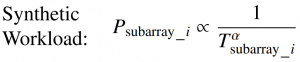
If the probability factor α is close to 0, it indicates a uniform workload. As α increases, there is more access to data closer to the array root pin. Thus, sweeping α provides an efficient way to quantify the potential advantages of E-Tree. Psubarray_i , Lsubarray_i , and Tsubarray_i are the access probability to subarray i , the length (in the space) and the delay (in the timing) of interconnect to subarray i from the array root pin, respectively. Accessbank_i is the total access number to the bank i. Realistic workloads of non-uniform are executed from SPEC CPU 2017, and a list of benchmarks is shown below:
| Benchmark | Benchmark Program General Category |
| 602.gcc | GNU C Language optimizing compiler |
| 605.mcf | Combinatorial Optimization & Vehicle Scheduling |
| 607.cactus | Physics: General/Numerical Relativity |
| 623.xalan | XSLT processor for transforming XML to HTML |
| 625.x264 | Video compression |
| 641.leela | AI: Go engine with Monte Carlo & selective tree search |
| 649.fotonik | Computational Electromagnetics (CEM) |
| 654.roms | Regional Ocean Modeling System |
Cache Design
| Parameter | Value | Explanation |
| -size (bytes) | 134217728 | |
| -UCA bank count | 16 | |
| -UCA vertical bank count | 4 | |
| -access mode (normal, sequential, fast) | “sequential” | Timing path: core-to-cache, tag array, and data array loop. |
| -tree_space_to_time | 0 | 1: adopt clock frequency for the interconnect; 0: not adopt. |
| -frequency_down |
0 | 0: no; 1: yes; 2: fix_max_clock_cycle for Lmax; 3: fix_max_clock_cycle for Laverage. |
| -max_benchmark_clock_frequency |
3e9 | |
| -max_clock_cycle |
1000 | Set the max clock cycle for the worst case of timing path or average length. |
| -max_clock_frequency |
3e9 | |
| -clock_frequency_factor | 1 | |
| -number_of_mats_shared_bits |
4 | Default value: 4. 2, 1. |
| -data_tag_ratio | 32 | Default value: 32. |
SRAM Subarray
| Parameter | Value | Explanation |
| -tag_array_overhead_with_min_or_max_delay | 2 | 1: Select a tag array with a min. delay; 2: select a tag array with a max. delay. |
| -SHD_SHP_SLP_DC_DAI | 0 | 0–6: Index of device and subarray design from IMEC, including standard design: 0 high density, 1 high performance, 2 low power; divided design: 3 conventional, 4 active interconnect A14, 5 active interconnect 22nm FDSOI, 6 A14 Si. |
| -SHD_sweep_a14_to_a3 | 0 | For high-density subarray, 0: A14, [128–1024]C×[128–512]R; 1: A14, A10, A5, and A3 for 288C×256R, 576C×128R. |
| -LBWL_per_subarray |
4 | Number of Local blocks of word line per subarray. |
| -LBBL_per_subarray | 8 | Number of Local blocks of bit line per subarray. |
| -multi_port | 0 | 0 or 1: Not multi-port; 2: dual-port; 4. |
Interconnect and Circuit
| Parameter | Value | Explanation |
| -htree_spacing_type | 2 | 0: Side-pin access; 1: Non-conventional (active) interconnect; 2: Center-pin access; 3: Non-conventional interconnect + Center-pin access. |
| -Wire signaling (fullswing, lowswing, default) | “Global_30” | Global_frequency_down & -dtl_core_to_cache 0: frequency down.
Global_30 & -dtl_core_to_cache 0: the cache adopts repeater insertion. lowswing & -dtl_core_to_cache 0: the cache adopts low swing. Fix_max_clock_cycle: fix max clock cycle for the worst case of timing path or average length. differential_transmission_line & -dtl_core_to_cache 1: the data array and core-to-cache adopt DTL. Global_30 & -dtl_core_to_cache 1: the data array adopts repeater insertion, core-to-cache adopts DTL. Global_30 & -dtl_core_to_cache 2: the data array intra-bank adopts repeater insertion, inter-bank and core-to-cache adopt DTL. |
| -dtl_core_to_cache |
2 | 0: the cache adopts repeater insertion. |
| -dtl_aspect_ratio |
2 | Data array DTL aspect ratio. |
| -force_bits | 0 | 0: The number of data and address bits is based on Cacti computation. 288: force the value as 288 by the user. |
| -delay_overhead | 0.3 | Global_30 & 0.3: Adopt Cacti repeater insertion interconnect circuit model based on the delay overhead of 30%; Global_30 & 1e12: low power; Global_30 & 1e15: adopt repeater insertion based on Spectre simulation. It is important to note that when comparing DTL with repeater insertion, the latter should be based on Spectre simulation in order to ensure consistency. |
| -Interconnect material | “cu” | Cu, graphene-capped Ru, graphene-capped Cu, thick graphene, combination of graphene-capped Cu and thick graphene. |
| -grain_eff | 3 | The grain effect factor for graphene-capped Cu. |
| -mfp_scale | 1 | The mean free path scale factor for graphene is as follows: As the factor increases, the resistance decreases. |
| -gracu_nlayer | 7 | The number of layers of graphene for graphene-capped Cu interconnect. |
| -graRcon0 | 100 | Graphene contact resistance, 100Ω⋅μm. |
| -wire_level | 5 | Interconnect metal layer. The geometry is based on the instructions from IMEC. |
| -output_wire_distribution | 0 | 1: output wire distributions, including wire length, delay, energy, access probability to each subarray for data array and tag array. |
| -imec_he_tree_array_level |
1 | 1: E-tree; 0: H-tree. Note: Array level interconnect technology is the same as the bank level counterpart. |
| -imec_he_tree_bank_level |
1 | 1: E-tree; 0: H-tree. This parameter is also described in Software Workload. |
| -probability_factor_Lw_n_exp | 5 | If value >= 0.1, Synthetic Workload; if value < 0.1, 0.0602, 0.0605, 0.0607, 0.0623, 0.0625, 0.0641, 0.0649, 0.0654: Realistic Workload, using corresponding *.txt, including the number of accesses to each bank, located within the current folder. E-Tree works for software workload. The parameter is described in Software Workload too. |
| -wire_core_to_cache_cu | 1 | 1: core-to-cache interconnect adopts Cu only; 0: core-to-cache interconnect uses the same material as the cache. |
| -wire_core_to_cache_width |
2 | Core-to-cache interconnect width, unit: μm. |
| -wire_core_to_cache_ar | 0.1 |
Technology Nodes and Device
| Parameter | Value | Explanation |
| -technology (u) | 0.0014 | Interconnect repeater technology node from IMEC. |
Target
| Parameter | Value | Explanation |
| -Optimize ED or ED^2 (ED, ED^2, NONE): | “ED” | ED: minimize EDP; EAD: minimize EDAP. |
/tech_params/*.dat
| Parameter | Explanation |
| -C_drain (F/um) | Repeater drain capacitance. |
| -C_gate (F/um) | Repeater gate capacitance. |
| -Vdd (V) | Supply voltage. |
| -Vth (V) | Threshold voltage. |
| -I_on_n (A/um) | The current required for the repeater to achieve the desired output resistance is referred to as the “repeater ON current.” |
| -I_off_n (A/um) | Leakage current under a variety of temperatures. |
| -I_g_on_n (A/um) | Gate leakage current under a variety of temperatures. |
| -area_cell (um^2) | Area of IMEC-designed subarray. |
|
-asp_ratio_cell
|
Aspect ratio of IMEC-designed subarray. |
| -imec_workload_I_on_n_drv (A/um) | This designation is reserved for non-conventional interconnects. |
| -imec_subarray_column_choice (s_J) | Number of columns of IMEC-designed subarray. |
| -imec_subarray_read_latency (s) | Read latency of IMEC-designed subarray. |
| -imec_subarray_write_latency (s) | Write latency of IMEC-designed subarray. |
| -imec_subarray_read_energy (J) | Read energy of IMEC-designed subarray. |
| -imec_subarray_write_energy (J) | Write energy of IMEC-designed subarray. |
| -wire_pitch (um) | Interconnect pitch. |
| -wire_width (um) | Interconnect width. |
| -barrier_thickness (um) | Cu interconnect barrier thickness. |
| -aspect_ratio (-) | Interconnect aspect ratio. |
Google Scholar, ORCID, ResearchGate. EndNote.
Selected Publications:
The corresponding Cacti++ papers and book in blue are as follows:
[18] Z. Pei*, S. Lu*, L. Shang, S. Jung, Q. Liang, and C. Pan, “Graphene-based interconnect exploration for FPGA design and optimization towards the end of the roadmap,” ACM Transactions on Design Automation of Electronic Systems, 2026. DOI: 10.1145/3810248
[17] Z. Pei, H.-H. Liu, M. Mayahinia, M. Tahoori, F. Catthoor, Z. Tokei, P. Dubey, and C. Pan, “Interconnect/Memory Co-Design and Co-Optimization Using Differential Transmission Lines,” IEEE Transactions on Very Large Scale Integration (VLSI) Systems, 2025. DOI: 10.1109/TVLSI.2025.3595818
[16] M. Mayahinia, T. Marinelli, Z. Pei, H.-H. Liu, C. Pan, Z. Tőkei, F. Catthoor, M.B. Tahoori, “System Scenario-based Design of the Last-Level Cache in Advanced Interconnect-Dominant Technology Nodes,” ACM Transactions on Embedded Computing Systems (TECS), 2025. DOI: 10.1145/3762649
[15] Z. Pei, H.-H. Liu, M. Mayahinia, M. B. Tahoori, F. Catthoor, Z. Tőkei, D. B. Abdi, J. Myers, and C. Pan, “Ultra-Scaled E-Tree-Based SRAM Design and Optimization With Interconnect Focus,” IEEE Transactions on Circuits and Systems I: Regular Papers, 2024. DOI: 10.1109/TCSI.2024.3438164
[14] M. Mayahinia, T. Marinelli, Z. Pei, H.-H. Liu, C. Pan, Z. Tokei, F. Catthoor, and M. B. Tahoori, “Dynamic Segmented Bus for Energy-efficient Last-level Cache in Advanced Interconnect-dominant Nodes“, IEEE Embedded Systems Letters, 2024. DOI: 10.1109/LES.2024.3444711
[13] H.-H. Liu, C. Gilardi, S. M. Salahuddin, Z. Pei, P. Schuddinck, Y. Xiang, P. Weckx, G. Hellings, M. G. Bardon, and J. Ryckaert, “Future Design Direction for SRAM Data Array: Hierarchical Subarray With Active Interconnect,” IEEE Transactions on Circuits and Systems I: Regular Papers, 2024. DOI: 10.1109/TCSI.2024.3410518
[12] H.-H. Liu, P. Schuddinck, Z. Pei, L. Verschueren, H. Mertens, S. M. Salahuddin, G. Hiblot, Y. Xiang, B. T. Chan, and S. Subramanian, “CFET SRAM With Double-Sided Interconnect Design and DTCO Benchmark,” IEEE Transactions on Electron Devices, 2023. DOI: 10.1109/TED.2023.3305322
[11] S. Lu, Z. Pei, L. Shang, S. Jung, Q. Liang, and C. Pan, “Graphene-Based FPGA Design and Optimization at the 7nm FinFET Technology Node“, in 2025 26th International Symposium on Quality Electronic Design (ISQED), 2025, pp. 1-7. DOI: 10.1109/ISQED65160.2025.11014392
[10] S. Lu, Z. Pei, L. Shang, S. Jung, and C. Pan, “A Technology/Circuit Co-design Framework for Emerging Reconfigurable Devices,” in 2023 IEEE 66th International Midwest Symposium on Circuits and Systems (MWSCAS), 2023, pp. 1123-1127. DOI: 10.1109/MWSCAS57524.2023.10406005
[9] Z. Pei, M. Mayahinia, H.-H. Liu, M. Tahoori, F. Catthoor, Z. Tokei, and C. Pan, “Technology/Memory Co-Design and Co-Optimization Using E-Tree Interconnect,” in Proceedings of the Great Lakes Symposium on VLSI 2023, 2023, pp. 159-162. DOI: 10.1145/3583781.3590311
[8] Z. Pei, M. Mayahinia, H.-H. Liu, M. Tahoori, S. M. Salahuddin, F. Catthoor, Z. Tokei, and C. Pan, “Emerging Interconnect Exploration for SRAM Application Using Nonconventional H-Tree and Center-Pin Access,” in 2023 24th International Symposium on Quality Electronic Design (ISQED), 2023, pp. 1-1. DOI: 10.1109/ISQED57927.2023.10129316
[7] Z. Pei, M. Mayahinia, H.-H. Liu, M. Tahoori, F. Catthoor, Z. Tokei, and C. Pan, “Graphene-Based Interconnect Exploration for Large SRAM Caches for Ultrascaled Technology Nodes,” IEEE Transactions on Electron Devices, vol. 70, pp. 230-238, 2022. DOI: 10.1109/TED.2022.3225512
[6] Z. Pei, F. Catthoor, Z. Tokei, and C. Pan, “Beyond-Cu Intermediate-Length Interconnect Exploration for SRAM Application,” IEEE Transactions on Nanotechnology, 2022. DOI: 10.1109/TNANO.2022.3157952
[5] Z. Pei, A. Dutta, L. Shang, S. Jung, and C. Pan, “Interconnect Technology/System Co-Optimization for Low-Power VLSI Applications Using Ballistic Materials,” IEEE Transactions on Electron Devices, vol. 68, pp. 3513-3519, 2021. DOI: 10.1109/TED.2021.3077210
[4] Z. Pei, L. Shang, S. Jung, and C. Pan, “Deep Pipeline Circuit for Low-Power Spintronic Devices,” IEEE Transactions on Electron Devices, vol. 68, pp. 1962-1968, 2021. DOI: 10.1109/TED.2021.3059601
[3] G. Jalilvand, O. Ahmed, K. Bosworth, C. Fitzgerald, Z. Pei, and T. Jaing, “Application of a metallic cap layer to control Cu TSV extrusion,” in 2017 IEEE 67th Electronic Components and Technology Conference (ECTC), 2017, pp. 61-66. DOI: 10.1109/ECTC.2017.290
[2] Y. Yuan, M. Du, S. Zhang, and Z. Pei, “Effects of BiNbO4 on the microstructure and dielectric properties of BaTiO3-based ceramics,” Journal of Materials Science: Materials in Electronics, vol. 20, pp. 157-162, 2009. DOI: 10.1007/s10854-008-9674-5
[1] Z. Pei, Y. Yuan, S. Zhang, and B. Li, “Studies on Fabrication and Properties of High Temperature Ceramic Capacitors Sintered at Intermediate Temperature,” Materials Reports: Special Issue on Nanomaterials and New Materials, issue 1, pp. 366–369, 2009. DOI: 10.3321/j.issn:1005-023X.2009.z1.108
*The macro-level data utilized in the research presented in the book was generated using Cacti++:
[*] H.-H. Liu and F. Catthoor, “Circuit-Technology Co-Optimization of SRAM Design in Advanced CMOS Nodes,” Springer, 2024. DOI: 10.1007/978-3-031-76109-6