Projects
SOME ACADEMIC PROJECTS ONLY
Business projects are not publicly available due to copyright and proprietary considerations.

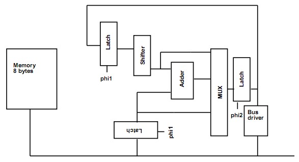
Design Digital VLSI Circuits Columbia Integrated Systems Laboratory, Columbia University, 2009 Design an 8-bit microcontroller core, implemented in TSMC CMOS process, Digital VLSI Circuits Designed an 8-bit microcontroller core to perform essential functions within the clock distribution system. Score: 95/100
- Project Overview: Completed a professional report under the guidance of Professor Kenneth L. Shepard, focusing on the design and implementation of a controller core.
- Tools and Platform: Utilized industry-standard EDA/CAD tools, including Cadence Composer, Virtuoso, Assura; Synopsys HSPICE, Nanosim; Mentor Calibre on a Linux OS platform. Designs were implemented in TSMC 250nm process, with clean DRC and LVS and final GDSII submission.
![]()
![]() This project employed industry-standard EDA/CAD tools from Cadence, Synopsys, and Mentor (acquired
This project employed industry-standard EDA/CAD tools from Cadence, Synopsys, and Mentor (acquired ![]() by Siemens in 2017) on the GNU/Linux OS:
by Siemens in 2017) on the GNU/Linux OS:
-
- Synopsys Nanosim for timing analysis
- Cadence Ultrasim for timing analysis (now)
- Cadence Composer for schematic entry
- Cadence Schematic Editor for schematic entry (now)
- Cadence Virtuoso for layout design
- Synopsys HSPICE for circuit simulation
- Cadence Spectre for circuit simulation (now)
- Mentor Calibre for layout verification
- Cadence Assura for extraction
- Siemens Calibre for extraction (now)
- Chip Functionality: Designed a controller to execute memory read/write operations, data transfers between internal and external buses, and arithmetic operations (add, subtract, multiply). Functional blocks included full adder, shifter, bus driver, decoder, memory, and PLAs.
- Physical Design Considerations: Addressed floorplanning, placement and routing (P&R, PnR), timing closure, congestion mitigation, power optimization, etc., throughout the design flow.
- Floorplan Strategy: Aligned dataflow signals horizontally and control signals vertically. Layer usage included vertical M1, horizontal M2, and M3 for power/ground distribution.
- Timing closure: Resolved setup violations by upsizing repeaters and shortening critical paths or repeater spacing; addressed hold violations with repeater insertion (buffers or inverters). It is important to note that the optimal repeater spacing exists to minimize the delay of interconnect with repeater insertion.
- Congestion Management: Handled localized routing congestion by refining the floorplan and preserving routing margins, avoiding increased die size or metal layers to control manufacturing cost and yield.
- Power Optimization: Applied multi threshold voltage (multi-Vt) design methodology. High-Vt transistors were used to reduce leakage, with low-Vt selectively applied to critical timing path. Final design minimized dynamic, switching, internal, and leakage power by balancing performance and power trade-offs.
- Glitch Prevention: Replaced latches with edge-triggered D flip-flops (DFFs) to prevent glitches from propagating to subsequent stages.
- Verification and Simulation: Verified functionality and timing through HSPICE and Nanosim simulation. Utilized a combination of HSPICE and Nanosim simulations to verify the clock cycle time, to calculate power dissipation. Used Programmer’s Hierarchical Interactive Graphics System (PHIGS) Extension to X (PEX) for parasitic extraction and logic verification, to verify that core and dataflow functional units were functionally correct. Leveraged Espresso to optimize PLA-based controller logic.
- CMOS VLSI Design A Circuits and Systems Perspective Fourth Edition
Senior Design Engineer | Cadence Design Systems, Inc., 2012~2016
- SoC Realization Group (renamed as IP Group in August 2013) R&D.
- Had extensive experience in the design flow of integrated circuits by designing DDR PHY IP in SoC.

-
- Platform: Linux OS. Scripting: Tcl, Shell, Perl, etc. The design standards covered performance, power, and area (PPA). Analyzed and debugged timing & physical violations. Submitted clean GDSII & files for signoff and tapeout (fabrication) of 15+ IP designs: netlist/gds/lib/lef/ctsmdl/spef/sdf/ctl/cdl, etc.
- Cadence® EDA tools: Innovus™ Implementation System, Encounter® Digital Implementation System (EDI), Tempus™, Encounter® Timing System (ETS), Genus™ Synthesis Solution, Encounter® RTL Compiler, Physical Verification System (PVS), Pegasus, Encounter® Power System, CMP Predictor, Litho Physical Analyzer (LPA), Conformal® Logic Equivalence Check (LEC), Quantus Extraction Solution, QuickView Signoff Data Analysis Environment, Voltus™ IC Power Integrity Solution, Spectre, (SPICE), Virtuoso, etc.
- Technology nodes: TSMC 16nm FinFET, 28HPM, 28HPC, 28LP, 40LP; GlobalFoundries 28SLP, 28LP, etc.
- Deeply understood RTL netlist synthesis and static timing analysis (STA) timing constraints. Clock tree synthesis (CTS) in CTS spec files or CCOpt based on the integrated circuit (IC) design, e.g., clock tree structure, critical path, and timing/skew criteria for timing closure in STA. Extensive knowledge of the critical path & timing closure challenges.
- Set MMMC library set, RC/delay corners, setup/hold analysis views based on release from foundries, involving *.lib (timing library), *.cdb (SI files), and files for RC parasitic extraction (tech files for QRC, SPEF, SDF, delay), operating conditions (best/worst corners, Process Voltage Temperature, PVT). Followed the guides/release of the foundries. Chose correct LEF/DEF/GDS/lib/Technology files, CDL, and other industry-standard data formats relevant to the instance, cell, D Flip-Flop (DFF), wire, power, and ground lib files, set On-Chip Variation (OCV) derating for the launch/capture path.
- Mastered physical design (PD, back-end) flow: floorplan, placed important instances/cells on the critical path based on STA timing/skew reports and design specs, CTS, placement and routing (P&R), timing ECOs, SPEF SDF back annotation STA ECOs. Hierarchical design with pinning and budgeting flows. Designed assemble hierarchy (flatten partition hierarchy) and power grid to optimize PPA. Skilled in ASIC low-power and logic designs.
- Well-versed in debugging timing violations: setup/hold/skew/transition/duty, considering OCV derating, Signal Integrity (SI), crosstalk, noise, Common Path Pessimism Removal (CPPR)/CRPR, etc. Proficient in physical verification: ANT/ DRC/LVS/ERC/LPA/CMP/DFM, design for yield, etc. Extensive knowledge in verifications and analysis, e.g., formal verification, physical verification, Conformal Low Power (CLP) verification, power analysis, EM and IR closure, etc.
Columbia Integrated Systems Laboratory, Columbia University, 2009
Design a broad-band amplifier circuit, Analog Electronic Circuits.
Score: 95/100
- Designed the project under the guidance of Professor Yannis P. Tsividis and submitted a summary of a comprehensive summary.
- Applied PSPICE to develop a broad-band amplifier circuit which met the requirements. Constructed and tested circuits on a breadboard using standard laboratory instruments.
- Developed a broad-band amplifier which meet voltage gain: more than 60 dB, pass-band: from ≤100 Hz to ≥100 kHz, frequency response variation: less than 3 dB within pass-band, total harmonic distortion with 4 V peak-to-peak output: < 1 % @ 1 KHz. Under operation environment: temperature range: 0 ~ 85 °C, supply voltage: 9 V ± 0.5 V (single), source resistance: 50 Ω, load resistance: 1 KΩ. Let supply current: as low as possible, used only a single power supply, resistors, capacitors, and 2N2222A transistors.
Ph.D. in Electrical Engineering, The University of Texas at Arlington (UTA), 2025
- Dissertation: “Emerging Energy-efficient Scalable Interconnect Design for VLSI Logic and Memory Applications”
- Official digital PhD diploma in Electrical Engineering
- Research: Modeling and optimization of energy-efficient computing systems, spanning from the hardware to the software, and leveraging emerging interconnect and device technologies at ultra-scaled advanced technology nodes.
- Research is funded by IMEC, DOE, and NSF.
-
- Engage in extensive collaboration with the Interuniversity Microelectronics Centre (IMEC) on developing and validating a framework, Cacti++, to address the existing gap at IMEC in the initial stages of system-level design for rapid verification & simulation of technology nodes, ranging from 5- to 14-Å-compatible technologies.
- Focus on technology/system co-design and interconnect technologies. Utilize Linux as the R&D platform, which is used to develop an executable tool Cacti++ in C++/makefile and to perform circuit simulations/synthesis in EDA/CAD tools, e.g., Cadence Spectre/Virtuoso/Innovus/Genus, Synopsys Hspice/Raphael/Design Compiler, etc.
- Establish a comprehensive co-design & co-optimization pathway by the Cacti++ framework, which bridges the gap from bottom-level technology/transistor/device/circuit, interconnect/fabric, & cache memory to top-level software. Apply Tcl, Matlab, & Slurm/sbatch automatically to sweep design parameters, spanning from technology to software.
- Provide researchers from imec and the partner universities with simulation results by Cacti++, e.g., PPA optimization/analysis, etc. The C++ code is accessible to them to support the further development of the tools.
- Deliver updates during virtual international meetings and support project progress with post-meeting follow-ups.
- Explore the Cacti++ framework and research contributions: https://blogs.cuit.columbia.edu/zp2130/cacti/ and https://blogs.cuit.columbia.edu/zp2130/publications.
- Graduate Teaching and Research Assistant, Grader: 2020.01~2025.05. Electronics, Circuits, and Circuits with Lab.
- Related courses: Robotics | Nonlinear Systems | Random Processes. GPA: 4.0/4.0.
- Related award: Dr. K. R. Rao Electrical Engineering Graduate Fellowship.
Design Electromigration (EM) Test Pad Layout, University of Central Florida
- Utilized Cadence® Virtuoso® to design layout for Electromigration (EM) Test Pad for tape-out with Harris Corporation and ICAMR in Fall 2016, partner was Novati Technologies, Inc. who I submitted GDSII to.
- Map file was from MOSIS: https://www.eda.ncsu.edu/wiki/MOSIS_Layers, https://eda.ncsu.edu/
- The test pad size: 120um x 120 um. Pitch: 250um, which means 130um spacing between 2 test pads, with maligned vias, or different numbers of links, or different trace widths.
- The stack-up was M1, DBI1, DBI2, M2. DBI1 and DBI2 are nominally identical, unless the designer wanted to intentionally misalign them.
- Virtuoso layout layers: metal 1 was the first-layer metal, via was metal1-metal2 contact, metal 2 was the second-layer metal, via2 was the metal2-metal3 contact, metal3 was the third metal. For EM Test Pad foundry, metal1 was for M1, via was for DBI1, metal2 was for DBI2, via 2 was for M2, and metal3 was for test pad.
Medical Device Modeling
Columbia Integrated Systems Laboratory, Columbia University, 2009
Maximizing Power Transfer to a Coaxial Antenna for Interstitial Microwave Hyperthermia, Circuit Theory.
Score: 80/100
- Conducted the design project under the mentorship of Professor Omar Wing and submitted a mid-term project report with the paper version.
- Microwave hyperthermia refers to a medical procedure in which microwave energy is delivered to cancerous tissues in an organ, in the hope that the energy would generate sufficient amount of heat to destroy the malignant tissues while the surrounding healthy tissues are unaffected.
- Collected relevant research references on one kind of medical Microwave Thermotherapy (Interstitial Microwave Hyperthermia) which cures tumor with a key component coaxial antenna. Analyzes and summarized relevant medical Microwave Thermotherapy and coaxial antenna power transfer theory and knowledge.
- Modeling human main organs tissues physical parameters, such as Conductivity, Thermal Conductivity, and Permittivity etc.
- Economical: According to relevant references, power transmission theory and the commercial point which maximized return on investment (ROI), coaxial antenna power transfer modeling, i.e. simple L, C two-port structure.
- Versatile: Considered variety main organs tissues and organ composition varies from patient to patient, microwave source work frequency 2.45 GHz sensitivity or stability engineering issues, optimized coaxial antenna power transfer model which was suitable for various organs.
- Maximizing Performance: Applied MATLAB to simulate coaxial antenna power transfer model, obtained a good modeling in which power transmission efficiency was 89-96 percents with different organs.
Columbia Integrated Systems Laboratory, Columbia University, 2009
Design a bandpass filter with band edge frequencies w1=pi/4 and w2=3pi/4, Digital Signal Processing.
Score: 250/250
- Completed the design project under Professor Xiaodong Wang‘s supervision and submitted a project summary.
- Utilized Matlab to develop and simulate using various methods.