Clock Tree Latency Skew Uncertainty
Clock to a SoC/chip is like blood to a dog body. If you want the pet smart and strong, hematological system would be healthy. Just the way blood flows to each and every part of the body and regulates metabolism, clock reaches each and every sequential device and controls the digital events inside the chip.
There are two phases in the design of a clock signal.
1st the clock is in “ideal mode” (e.g.: during RTL design, during synthesis and during placement). An “ideal” clock has no physical distribution tree, it just shows up magically on time at all the clock pins.
2nd phase comes when clock tree synthesis (CTS) inserts an actual tree of buffers into the design that carries the clock signal from the clock source pin to the (thousands/millions) of flip-flops that need to get it. CTS is done after placement and before routing. After CTS is finished, the clock is said to be in “propagated mode”.
What is clock latency?
Clock latency is an ideal mode term. It refers to the delay that is specified to exist between the source of the clock signal and the flip-flop clock pin. This is a delay specified by the user – not a real, measured thing. When the clock is actually created, then that same delay is now referred to as the “insertion delay”. Insertion delay (ID) is a real, measurable delay path through a tree of buffers. Sometimes the clock latency is interpreted as a desired target value for the insertion delay.
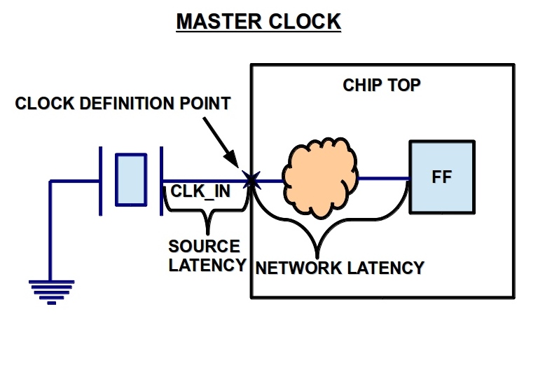
Clock latency is the time taken by the clock to reach the sink pin from the clock source. It is divided into two parts – Clock Source Latency and Clock Network Latency. Clock Source Latency defines the delay between the clock waveform origin point to the definition point. Clock Network Latency is the delay form the clock definition point to the sink pin. Clock Latency is also called Clock Insertion Delay. Please see the below 2 pictures to get a better understanding of what Clock Latency is.

create_clock [get_ports clk_phy ] -name clk_phase_0 -period 1.874 -waveform "0 0.5*1.874"
set_clock_uncertainty -setup $SKEW_MAX [get_clocks clk_phase_0]
set_clock_uncertainty -hold $SKEW_MIN [get_clocks clk_phase_0]
create_generated_clock -name slice_clk_ctlr_phase_0 -divide_by 2 -add \
-source [get_ports clk_phy] \
-master [get_clock clk_phase_0] \
[get_pin inst_clk_div/inst_clk_div_dff/hic_dnt_div_flop/Q]
set_clock_uncertainty -setup $SKEW_MAX [get_clock slice_clk_ctlr_phase_0]
set_clock_uncertainty -hold $SKEW_MIN [get_clock slice_clk_ctlr_phase_0]
create_clock dqs_ipad[0] -name read_mem_dqs_phase_0 -period 1.784 -waveform "0 0.5*1.784"
set_clock_uncertainty -setup $SKEW_READ_DQS_MAX [get_clock read_mem_dqs_phase_0]
set_clock_uncertainty -hold $SKEW_READ_DQS_MIN [get_clock read_mem_dqs_phase_0]
create_generated_clock -name delayed_dqs_phase_1 -source dqs_ipad[0] \
 -edges {1 2 3} -edge_shift "0.25*1.874 0.25*1.874 0.25*1.874" \
 -add -master_clock [get_clocks read_mem_dqs_phase_0] dll/dll_delay_line_rd_dqs/delay_0/r1/hic_dnt_dll_nand2/A1

delayed_dqs_phase_1 is dqs_ipad[0] shift 0.25 clock cycle
Path 1: MET Setup Check with Pin dfi_read_datablk/read_datablk_fifo/io_datain_l_reg_0_/CP

Endpoint: dfi_read_datablk/read_datablk_fifo/io_datain_l_reg_0_/D (v) checked with leading edge of 'clk_phase_0'

Beginpoint: dfi_read_datablk/read_datablk_fifo/dll_entry_flop_l_40/hic_dnt_dll_entry_flop/Q (v) triggered by leading edge of 'delayed_dqs_phase_1'

Path Groups: {reg2reg}
Other End Arrival Time 0.462
- Setup 0.099
+ Path Delay 0.901
+ Path Ideal Arrival 0.468
+ CPPR Adjustment 0.000
- Uncertainty 0.050
= Required Time 1.683
- Arrival Time 1.674
= Slack Time 0.009
 Clock Rise Edge 0.000
 = Beginpoint Arrival Time 0.000

 dqs_ipad[0] dqs_ipad[0] ^ 0.000 0.150 0.004 2
...
 dfi_dqs_in/hic_dll_dqs_mod_dqs0/hic_dnt_dll_dqs_not/ZN
 I v -> ZN ^
 CKND8BWP12T35P140 0.037 0.218 0.000 0.016 0.007 1.039
 dll/dll_delay_line_rd_dqs/delay_0/r1/hic_dnt_dll_nand2/A1
 CKND2D1BWP12T35P140
 0.001 0.687 0.000 0.016 0.007 2 1.000 delayed_dqs_phase_1 Adj. = 0.468
...
 dfi_read_datablk/read_datablk_fifo/dll_entry_flop_l_40/hic_dnt_dll_entry_flop/CP
 EDFQD2BWP12T35P140
 0.005 0.957 0.002 0.019 0.027 11 1.000
 dfi_read_datablk/read_datablk_fifo/dll_entry_flop_l_40/hic_dnt_dll_entry_flop/Q
 CP ^ -> Q v EDFQD2BWP12T35P140
 0.112 1.069 0.000 0.012 0.002 1.077
...
What is clock skew?
Clock Skew between two sink pins is the the difference in the clock latency between them. If the capture clock latency is more than the launch clock, then it is positive skew. This helps setup checks. If the capture clock latency is less than the launch clock, then it is negative skew. This helps hold checks. Ideal clock skew in a design is zero which is not achieveable. Clock tree is built to reduce the clock skew values.
What is clock uncertainty?
Clock uncertainty is the deviation of the actual arrival time of the clock edge with respect to the ideal arrival time. In ideal mode the clock signal can arrive at all clock pins simultaneously. But in fact, that perfection is not achievable. So, to anticipate the fact that the clock will arrive at different times at different clock pins, the “ideal mode” clock assumes a clock uncertainty. For example, a 1 ns clock with a 100 ps clock uncertainty means that the next clock tick will arrive in 1 ns plus or minus 50 ps.
A deeper question gets into why the clock does not always arrive exactly one clock period later. There are several possible reasons but here will list 3 major ones:
(a) The insertion delay to the launching flip-flop’s clock pin is different than the insertion delay to the capturing flip-flop’s clock pin (one paths through the clock tree can be longer than another path). This is called clock skew.
(b) The clock period is not constant. Some clock cycles are longer or shorter than others in a random fashion. This is called clock jitter which can be contributed from PLL or crystal osillator, cables, transmitters, receivers, internal circuitry of the PLL, thermal noise of the osillator etc. In the case of Pre CTS, since clock tree is not built, uncertainty = skew + jitter . Post CTS uncertainty = jitter .
(c) Even if the launching clock path and the capturing clock path are absolutely identical, their path delays can still be different because of on-chip variation (OCV). This is where the chip’s delay properties vary across the die due to process variations or temperature variations or other reasons. This essentially increases the clock skew.

Comments
So empty here ... leave a comment!