Configure STA environment
- What’s STA environment?
- Specifying Clocks. Clock uncertainty and Clock latency
- Generated clocks
- Input paths constraint
- Output paths constraint
- Timing path groups
- External attributes modeling
- Check design rules
- Refine timing analysis
- Point-to-point specification
Set up environment for static timing analysis. Specification of correct constraints is important in analyzing STA results. Design environment should be specified accurately so that STA analysis can identify all the timing issues in the design. Preparing for STA, setting up clocks, specifying IO timing characteristics, and specifying false paths and multicycle paths.
1. What’s STA environment?
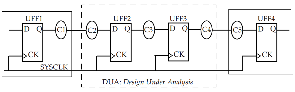
Figure 1 A synchronous design
Most digital designs are synchronous where the data computed from previous clock cycle is latched in the flip-flops at the active clock edge. Consider a typical synchronous design shown in Figure 1. It is assumed that Design Under Analysis (DUA) interacts with other synchronous designs. This means that DUA receives data from a clocked flip-flop and outputs data to another clocked flip-flop external to DUA.
To perform STA on this design, one needs to specify clocks to the flip-flops, and timing constraints for all path leading into the design and for all paths exiting the design.
Example in Figure 1 assumes that there is only one clock and C1, C2, C3, C4, and C5 represent combination blocks. The combination blocks C1 and C5 are outside of the design being analyzed.
In a typical design, there can be multiple clocks with many paths from one clock domain to another. The following sections describe how the environment is specified in such scenarios.
2. Specifying Clocks
To define a clock, we need to provide the following information:
i. Clock source: it can be a port of design, or be a pin of a cell inside design (typically that is a part of a clock generation logic).
ii. Period: time period of clock.
iii. Duty cycle: high duration (positive phase) and low duration (negative phase).
iv. Edge times: times for rising edge and falling edge.
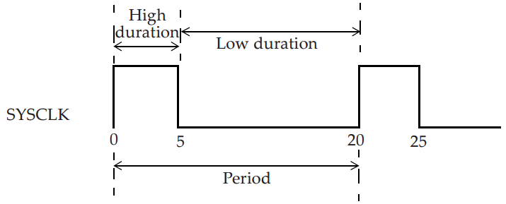
Figure 2 A clock definition
Figure 2 shows basic definitions. By defining clocks, all the internal timing paths (all flip-flop to flip-flop paths) are constrained; this implies that all internal paths can be analyzed with just the clock specifications. The clock specification specifies that a flip-flop to flip-flop path must take one cycle. We shall later describe how this requirement (of one cycle timing) can be relaxed.
Here is a basic clock specification.
create_clock \
-name SYSCLK \
-period 20 \
-waveform { 0 5 } \
[get_ports SCLK]
The name of the clock is SYSCLK and is defined at the port SCLK. The period of SYSCLK is specified as 20 units – the default time unit is nanoseconds if none has been specified. (In general, time unit is specified as part of technology library.) The first argument in waveform specifies time at which rising edge occurs and the second argument specifies time at which falling edge occurs.
There can be any number of edges specified in a waveform option, however, all edges must be within one period. The edge times alternate starting from the first rising edge after time zero, then a falling edge, then a rising edge, and so on. This implies that all time values in the edge list must be monotonically increasing.
-waveform {time_rise time_fall time_rise time_fall ... }
In addition, there must be an even number of edges specified. The waveform option specifies waveform within one clock period, which then repeats itself.
If no waveform option is specified, default is:
-waveform { 0 , period/2 }
Here is an example of a clock specification with no waveform specification.
create_clock -period 5 [ get_ports SCAN_CLK ]
In this specification, since no -name option is specified, the name of clock is the same as the name of the port, which is SCAN_CLK.
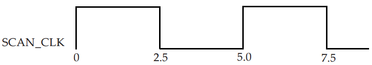 Figure 3 Clock specification example
Here is another example of a clock specification in which the edges of the waveform are in the middle of a period.
create_clock -name BDYCLK -period 15 \
-waveform { 5 12 } [get_ports GBLCLK]
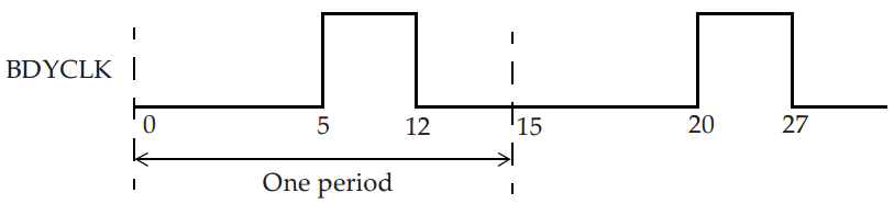 Figure 4 Clock specification with arbitrary edges
The name of the clock is BDYCLK and it is defined at the port GBLCLK. In practice, it is a good idea to keep the clock name the same as the port name.
Here are some more clock specifications.
# See Figure 5a:
create_clock -period 10 -waveform { 5 10 } [get_ports FCLK]
# Creates a clock with the rising edge at 5ns and the falling edge at 10ns.

# See Figure 5b:
create_clock -period 125 \
-waveform { 100 150 } [get_ports ARMCLK]
# Since the first edge has to be rising edge,
# the edge at 100ns is specified first and then the falling
# edge at 150ns is specified. The falling edge at 25ns is
# automatically inferred.
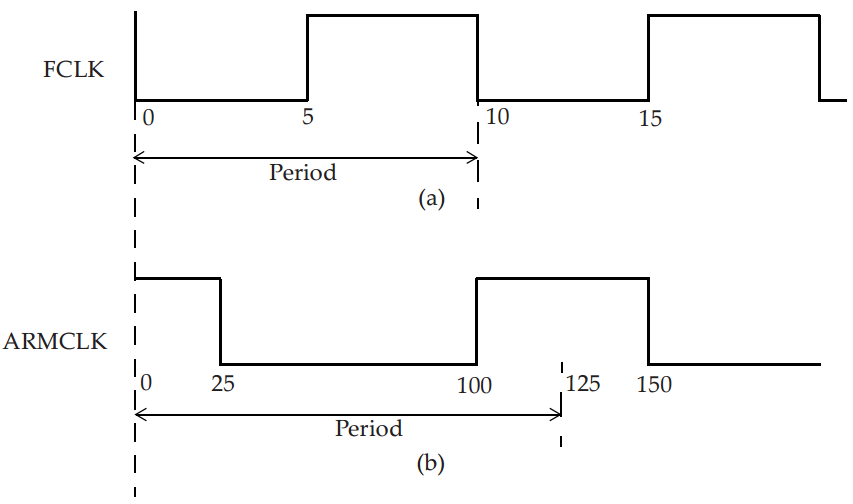 Figure 5 Example clock waveform
# See Figure 6a:
create_clock -period 1.0 -waveform { 0.5 1.375 } MAIN_CLK
# The first rising edge and the next falling edge is
# specified. Falling edge at 0.375ns is inferred
# automatically.

# See Figure 6b:
create_clock -period 1.2 -waveform { 0.3 0.4 0.8 1.0 } JTAG_CLK
# Indicates a rising edge at 300ps, a falling edge at 400ps
# a rising edge at 800ps and a falling edge at 1ns, this
# pattern is repeated every 1.2ns.
 Figure 6 Example with general clock waveform
2.1 Clock uncertainty
The timing uncertainty of a clock period can be specified using the set_clock_uncertainty specification. The uncertainty can be used to model various factors that can reduce the effective clock period. These factors can be the clock jitter and any other pessimism that one may want to include for timing analysis.
set_clock_uncertainty -setup 0.2 [get_clocks CLK_CONFIG]
set_clock_uncertainty -hold 0.05 [get_clocks CLK_CONFIG]
Note that clock uncertainty for setup effectively reduces available clock period by specified amount as illustrated in Figure 7. For hold checks, clock uncertainty for hold is used as an additional timing margin that needs to be satisfied.
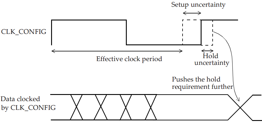 Figure 7 Specifying clock uncertainty
The following commands specify uncertainty to be used on paths crossing specified clock boundaries, called inter-clock uncertainty.
set_clock_uncertainty -from VIRTUAL_SYS_CLK -to SYS_CLK \
-hold 0.05
set_clock_uncertainty -from VIRTUAL_SYS_CLK -to SYS_CLK \
-setup 0.3
set_clock_uncertainty -from SYS_CLK -to CFG_CLK -hold 0.05
set_clock_uncertainty -from SYS_CLK -to CFG_CLK -setup 0.1
Figure 8 shows a path between two different clock domains, SYS_CLK and CFG_CLK. Based on the inter-clock uncertainty specifications above, 100ps is used as an uncertainty for setup checks and 50ps is used as an uncertainty for hold checks.
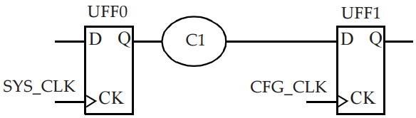 Figure 8 Inter-clock paths
2.2 Clock latency
Latency of a clock can be specified using the set_clock_latency command.
# Rise clock latency on MAIN_CLK is 1.8ns:
set_clock_latency 1.8 -rise [get_clocks MAIN_CLK]
# Fall clock latency on all clocks is 2.1ns:
set_clock_latency 2.1 -fall [all_clocks]
# The -rise, -fall refer to the edge at the clock pin of a # flip-flop.
There are two types of clock latency: network latency and source latency. Network latency is the delay from clock definition point (create_clock) to clock pin of a flip-flop. Source latency, also called insertion delay, is the delay from clock source to clock definition point. Source latency could represent either on-chip or off-chip latency. Figure 9 shows both the scenarios. The total clock latency at the clock pin of a flip-flop is the sum of source and network latency.
Here are some example commands that specify source and network latency.
# Specify a network latency (no -source option) of 0.8ns
# for rise, fall, max and min:
set_clock_latency 0.8 [get_clocks CLK_CONFIG]
# Specify a source latency:
set_clock_latency 1.9 -source [get_clocks SYS_CLK]
# Specify a min source latency:
set_clock_latency 0.851 -source -min [get_clocks CFG_CLK]
# Specify a max source latency:
set_clock_latency 1.322 -source -max [get_clocks CFG_CLK]
 Figure 9 Clock latency
3. Generated clocks
A generated clock is a clock derived from a master clock. A master clock is a clock defined using the create_clock specification.
When a new clock is generated in a design that is based on a master clock, the new clock can be defined as a generated clock. For example, if there is a divide-by-3 circuitry for a clock, one would define a generated clock definition at the output of this circuitry. This definition is needed as STA does not know that the clock period has changed at the output of the divide-by logic, and more importantly what the new clock period is. Figure 10 shows an example of a generated clock which is a divide-by-2 of the master clock, CLKP.
create_clock -name CLKP 10 [get_pins UPLL0/CLKOUT]
# Create a master clock with name CLKP of period 10ns
# with 50% duty cycle at the CLKOUT pin of the PLL.
create_generated_clock -name CLKPDIV2 -source UPLL0/CLKOUT -divide_by 2 [get_pins UFF0/Q]
# Creates a generated clock with name CLKPDIV2 at the Q
# pin of flip-flop UFF0. The master clock is at the CLKOUT
# pin of PLL. Period of generated clock is double that of
# clock CLKP, that is, 20ns.
 Figure 10 Generated clock at output of divider
Can a new clock (a master clock) be defined at the output of flip-flop instead of a generated clock? The answer is yes, however, there are some disadvantages. Defining a master clock instead of a generated clock creates a new clock domain. This is not a problem in general except that there are more clock domains to deal with in setting up the constraints for STA. Defining the new clock as a generated clock does not create a new clock domain, and generated clock is considered to be in phase with its master clock. The generated clock does not require additional constraints to be developed. Thus, one must attempt to define a new internally generated clock as a generated clock instead of set it as another master clock.
Another important difference between a master clock and a generated clock is the notion of clock origin. In a master clock, the origin of the clock is at the point of definition of the master clock. In a generated clock, the clock origin is that of the master clock and not that of the generated clock. This implies that in a clock path report, the start point of a clock path is always the master clock definition point. This is a big advantage of a generated clock over defining a new master clock as the source latency is not automatically included for the case of a new master clock.
Figure 11 shows an example where the clock SYS_CLK is gated by the output of a flip-flop. Since the output of the flip-flop may not be a constant, one way to handle this situation is to define a generated clock at the output of the and cell which is identical to the input clock.
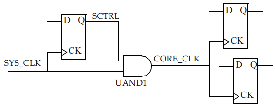
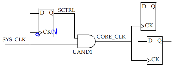 Figure 11 Clock gated by a flip-flop*
* It might be CKN in left FF, or it would not meet clock gating hold requirement, details and explain in Check clock gating
create_clock 0.1 [get_ports SYS_CLK]
# Create a master clock of period 100ps with 50% duty
# cycle.
create_generated_clock -name CORE_CLK -divide_by 1 \
-source SYS_CLK [get_pins UAND1/Z]
# Create a generated clock called CORE_CLK at the output of
# the AND cell and the clock waveform is the same as that
# of the master clock.
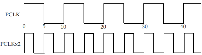 Figure 12 Master clock and multiply-by-2 generated clock
create_clock -period 10 -waveform { 0 5 } [get_ports PCLK]
# Create a master clock with name PCLK of period 10ns
# with rise edge at 0ns and fall edge at 5ns.
create_generated_clock -name PCLKx2 \
-source [get_ports PCLK] \
-multiply_by 2 [get_pins UCLKMULTREG/Q]
# Creates a generated clock called PCLKx2 from the master
# clock PCLK and the frequency is double that of the master
# clock. The generated clock is defined at the output of
# the flip-flop UCLKMULTREG.
Note that -multiply_by and -divide_by options refer to frequency of clock, even though a clock period is specified in a master clock definition.
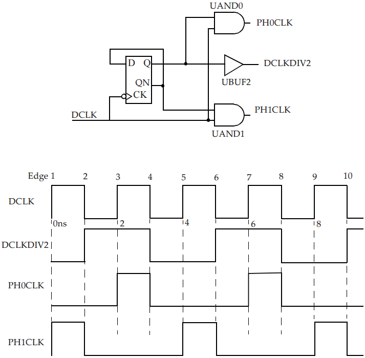 Figure 13 Clock generation
Figure 13 shows an example of generated clocks. A divide-by-2 clock in addition to out-of-phase clocks are generated. The waveform for clocks are also shown in figure.
create_clock 2 [get_ports DCLK]
# Name of clock is DCLK, has period of 2ns with a rise edge
# at 0ns and a fall edge at 1ns.
create_generated_clock -name DCLKDIV2 -edges {2 4 6}\
-source DCLK [get_pins UBUF2/Z]
create_generated_clock -name PH0CLK -edges {3 4 7} \
-source DCLK [get_pins UAND0/Z]
create_generated_clock -name PH1CLK -edges {1 2 5} \
-source DCLK [get_pins UAND1/Z]
Clock Latency for Generated Clocks
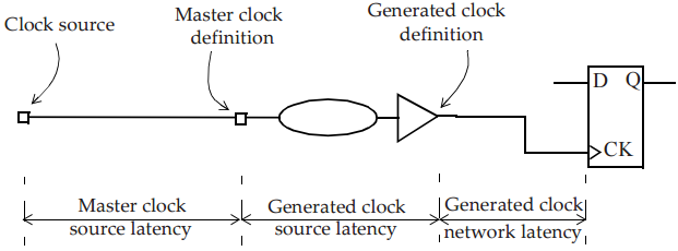 Figure 14 Latency on generated clock
A generated clock can have another generated clock as its source, that is, one can have generated clocks of generated clocks, and so on, however, a generated clock can have only one master clock.
Typical Clock Generation Scenario
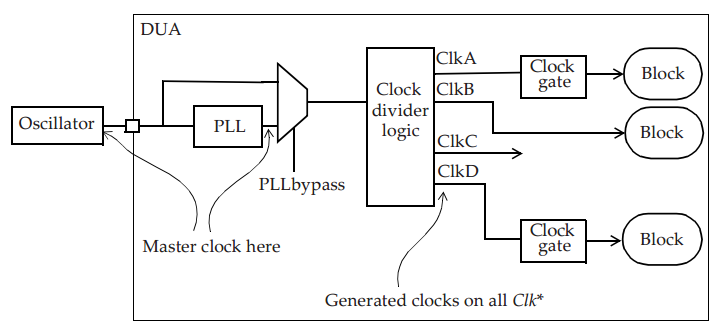 Figure 15 Clock distribution in a typical ASIC
Figure 15 shows a scenario of how a clock distribution may appear in a typical ASIC. The oscillator is external to the chip and produces a low frequency (10-50 MHz typical) clock which is used as a reference clock by on-chip PLL to generate a high-frequency low-jitter clock (200-800 MHz typical). This PLL clock is then fed to a clock divider logic that generates required clocks for ASIC.
On some of the branches of the clock distribution, there may be clock gates that are used to turn off the clock to an inactive portion of design to save power when necessary. PLL can also have a multiplexer at its output so that the PLL can be bypassed if necessary. A master clock is defined for the reference clock at the input pin of chip where it enters the design, and a second master clock is defined at the output of PLL. PLL output clock has no phase relationship with reference clock. Therefore, output clock should not be a generated clock of reference clock. Most likely, all clocks generated by the clock divider logic are specified as generated clocks of the master clock at PLL output.
4. Input paths constraint
STA cannot check any timing on a path that is not constrained. Thus, all paths should be constrained to enable their analysis.
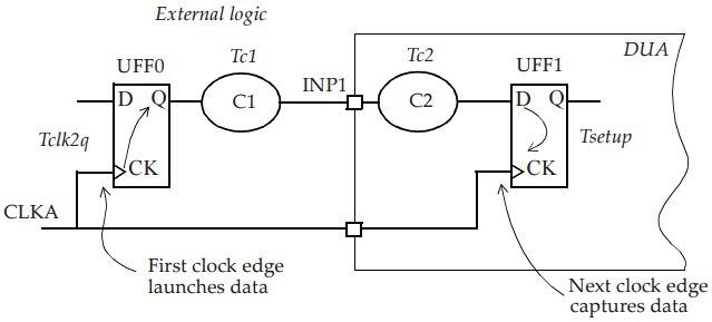 Figure 16 Input port timing path
Figure 16 shows an input path of Design Under Analysis (DUA). Flip-flop UFF0 is external to DUA and provides data to flip-flop UFF1 which is internal to DUA. Data is connected through input port INP1.
set Tclk2q 0.9
set Tc1    0.6
set_input_delay -clock CLKA -max [expr Tclk2q + Tc1]\
[get_ports INP1]
The constraint specifies that external delay on input INP1 is 1.5ns and this is with respect to clock CLKA. (in fact, input_delay equals to one part of data_path delay). Assuming clock period for CLKA is 2ns, then logic for INP1 pin has only 500ps (=2ns – 1.5ns) available for propagating internally in DUA. Tc2 + Tsetup <= 500ps for flip-flop UFF1 to reliably capture data launched by flip-flop UFF0.
5. Output paths constraint
Example A
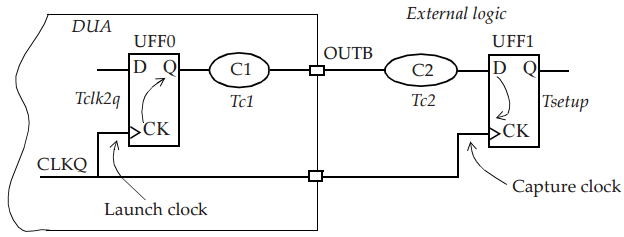 Figure 17 Output timing path
set Tc2  3.9
set Tsetup 1.1
set_output_delay -clock CLKQ -max [expr Tc2 + Tsetup] \
[get_ports OUTB]
Example B
 Figure 18 Output timing path Max Min delays
Tc2max + Tsetup = 7ns + 0.4ns = 7.4ns
Tc2min – Thold = 0 – 0.2ns = 0.2ns
create_clock -period 20 -waveform {0 15} [get_ports CLKQ]
set_output_delay -clock CLKQ -min -0.2 [get_ports OUTC]
set_output_delay -clock CLKQ -max 7.4 [get_ports OUTC]
Example C
 Figure 19 Input and output timing path
create_clock -period 100 -waveform {5 55} [get_ports MCLK]
set_input_delay 25 -max -clock MCLK [get_ports DATAIN]
set_input_delay 5 -min -clock MCLK [get_ports DATAIN]
set_output_delay 20 -max -clock MCLK [get_ports DATAOUT]
set_output_delay -5 -min -clock MCLK [get_ports DATAOUT]
6. Timing path groups
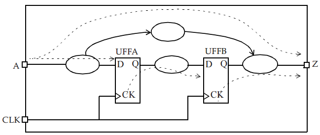 Figure 20 Timing paths
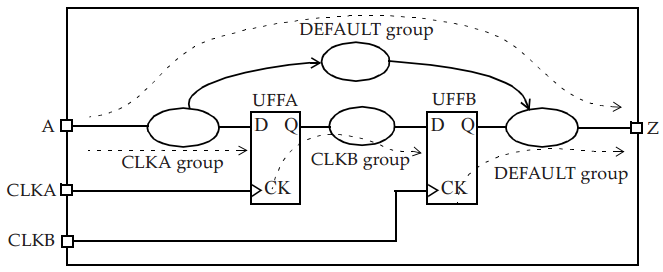 Figure 21 Path groups
Timing paths in a design can be considered as a collection of paths. Each path has a startpoint and an endpoint.
In STA, paths are timed based on valid startpoints and valid endpoints. Valid startpoints are: input ports and clock pins of synchronous device, such as flip-flops and memories. Valid endpoints are output ports and data input pins of synchronous devices. Thus, a valid timing path can be:
i. an input port —> an output port,
A —> Z
ii. an input port —> a data input pin of a flip-flop (FF) or a memory,
A —> UFFA/D
iii. a clock pin of FF —> a data input of FF,
UFFA/CLK —> UFFB/D
iv. a clock pin of FF —> an output port,
UFFB/CLK —> Z
Timing paths are sorted into path groups by the clock associated with endpoint of the path. Thus, each clock has a set of paths associated with it. There is also a default path group that includes all non-clocked (asynchronous) paths.
- CLKA group: A —> UFFA/D.
- CLKB group: UFFA/CK —> UFFB/D.
- DEFAULT group: A —> Z, UFFB/CK —> Z.
7. External attributes modeling
While create_clock, set_input_delay and set_output_delay are enough to constrain all paths in a design for performing timing analysis, these are not enough to obtain accurate timing for IO pins of block. The following attributes are required to accurately model environment of a design also. For inputs, one needs to specify slew at input. This information can be provided using:
- set_driving_cell
- set_input_transition
For outputs, one need to specify capacity load seen by output. This is specified by using following specification:
- set_load
![]() Figure 22 set_input_transition specification representation
Figure 22 set_input_transition specification representation
set_input_transition 0.85 [get_ports INPC]
# Specifies an input transition of 850ps on port INPC.
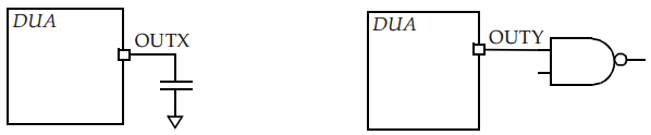 Figure 23 Capacity load on output port
set_load 5 [get_ports OUTX]
# Place a 5pF load on output port OUTX
The set_load specification can be used for specifying a load on an internal net in design.
set_load 0.25 [get_nets UCNT5/NET6]
# Set net capacitance to be 0.25pF.
8. Check design rules
Two of frequently used design rules for STA are max transition and max capacitance. These rules check all ports and pins in design meet specified limits for transition time and capacitance.
- set_max_transition
- set_max_capacitance
9. Refine timing analysis
Four common commands that are used to constrain analysis are:
i. set_case_analysis: Specify constant value on a pin of a cell, or on an input port.
ii. set_disable_timing: Break a timing arc of a cell.
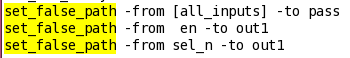
iii. set_false_path: Specify paths that are not real which implies that these paths are not checked in STA.
iv. set_multicycle_path: Specify paths that can take longer than one clock cycle.
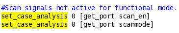
9.1 Specify inactive signals
In a design, certain signals have a constant value in a specific mode of chip. For example, if a chip has DFT logic in it, then Scan pin of chip should be at 0 in normal functional mode.
9.2 Break timing arcs in cells
Apply set_disable_timing to break timing arcs, for example, timing arcs in delay element is not real timing path in DDR PHY dataslice level STA.
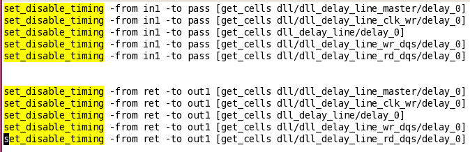
Note, One should caution when apply set_disable_timing as it removes all timing paths through specified pins. Where possilbe, it is preferable to apply set_false_path and set_case_analysis commands.
In fact, set_false_path is available for replacing set_disable_timing in some situation. For example, set_false_path during delay_element hardening, so it is no need to set_disable_timing in data_slice level after set_false_path in delay_element hardening.
9.3 Multicycle paths
In some case, data path between two flip-flops might take more than one clock cycle to propagate through logic. In such cases, this combination data path is declared as a multicycle path. Even though data is captured by capture FF on every clock edge, we direct STA that relevant capture edge occurs after specified number of clock cycles.
 Figure 24 A three-cycle multicycle path
Figure 24 shows an example, since data path takes 3 clock cycles, a setup multicycle check of 3 cycles should be specified. Multicycle setup constraints specified are given below.
create_clock -name CLKM -period 10 [get_ports CLKM]
set_multicycle_path 3 -setup \
-from [get_pins UFF0/Q] \
-to [get_pins UFF1/D]
A hold multicycle check should be checked as it was in a single cycle setup case, which is the one shown in Figure 24. It ensures that data is free to change anytime between 3 cycles. In absence of such a hold multicycle specification, default hold check is done on active edge prior to setup capture edge which is not intent. We need to move hold check 2 cycles prior to default hold check edge and hence a hold multicycle of 2 is specified. The intended behavior is shown in Figure 25.
set_multicycle_path 2 -hold \
-from [get_pins UFF0/Q] \
-to [get_pins UFF1/D]
 Figure 25 Hold check moved back to launch edge
The number of cycles denoted on a multicycle hold specifies how many clock cycles to move back from its default hold check edge which is one active edge prior to setup capture edge.
In most designs, if max path (or setup) requires N clock cycles, it is not feasible to achieve min path constraint to greater than (N-1) clock cycles.
Thus, in most designs, a multicycle setup specified as N cycles should be accompanied by a multicycle hold constraint specified as N-1 cycles.
10. Point-to-point specification
set_min_delay
set_max_delay
###########################################
### clk --> read_mem_dqs
###########################################
set_max_delay [expr ($PHY_THREEQUARTER - $skew_clk_to_read_mem_dqs_max)] -from [get_clock clk_phase_0] -to [get_clock read_mem_dqs*_phase_0]
set_min_delay [expr ($PHY_THREEQUARTER - $PHY_CLK_PERIOD + $skew_clk_to_read_mem_dqs_min)] -from [get_clock clk_phase_0] -to [get_clock read_mem_dqs*_phase_0]
Does delay in set_max/min_delay refer to source clock latency vs target clock latency skew? or data path delay?
Comments
So empty here ... leave a comment!