Crosstalk delay
Basics
Capacitance extraction for a typical net in a nanometer design consists of contributions from many neighboring conductors. Some of these are grounded capacitance while many others are from traces which are part of other signal nets. The grounded as well as inter-signal capacitance are illustrated in Figure 1.
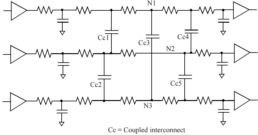 Figure 1 Example of coupled interconnect
All of these capacitance are considered as part of total net capacitance during basic delay calculation (without considering any crosstalk). When neighboring nets are steady (or not switching), inter-signal capacitance can be treated as grounded. When a neighboring net is switching, charging current through coupling capacitance impacts timing of the net. The equivalent capacitance seen from a net can be larger or smaller based upon direction of aggressor net switching. This is explained in a simple example below.
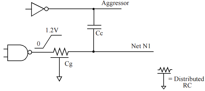 Figure 2 Crosstalk impact example
Figure 2 shows net N1 which has a coupling capacitance Cc to a neighboring net (labeled Aggressor) and a capacitance Cg to ground. This example assumes that net N1 has a rising transition at output and considers different scenarios depending on whether or not aggressor net is switching at the same time.
The capacitive charge required from driving cell in various scenarios can be different as described next.
i. Aggressor net steady. Driving cell for net N1 provides charge for Cg and Cc to be charge to Vdd. Total charge provided by driving cell of this net is thus (Cg + Cc) * Vdd. Base delay calculation obtains delay for this scenario where no crosstalk is considered from aggressor nets. Table 1 shows charge on Cg and Cc before and after switching of N1 for this scenario.
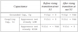 Table 1 Base delay calculation – no crosstalk
ii. Aggressor switching in same direction. Driving cell is aided by aggressor switching in the same direction. If aggressor transitions at the same time with the same slew (identical transition time), total charge provided by driving cell is only (Cg * Vdd). If slew of aggressor net is faster than that of N1, actual charge required can be even smaller than (Cg * Vdd) since aggressor net can provide charging current for Cg also. Thus, required charge from driving cell with aggressor switching in same direction is smaller than corresponding charge for steady aggressor described in Table 1. Therefore, aggressor switching in the same direction results in a smaller delay for switching net N1; the reduction in delay is labeled as negative crosstalk delay. See Table 2. This scenario is normally considered for min path analysis.
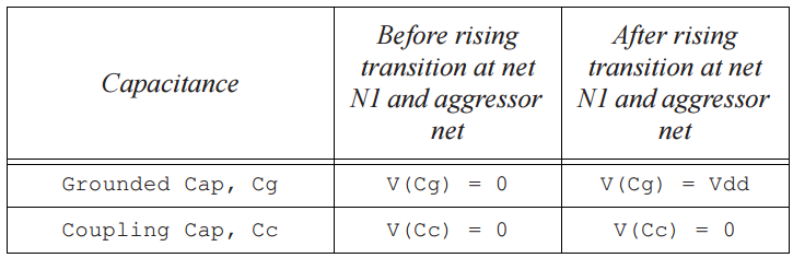 Table 2 Aggressor switching in same direction – negative crosstalk
iii. Aggressor switching in opposite direction. Coupling capacitance is charged from -Vdd to Vdd. Thus, charge on coupling capacitance change by (2 * Cc * Vdd) before and after transitions. This additional charge is provided by both driving cell of net N1 as well as aggressor net. This scenario results in a larger delay for switching net N1; increase in delay is labeled as positive crosstalk delay. See Table 3. This scenario is normally considered for max path analysis.
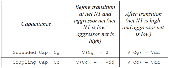 Table 3 Aggressor switching in opposite direction – positive crosstalk
Example above illustrates charging of Cc in various cases and how it can impact delay of switching net (labelled as N1). Example considers only a rising transition at net N1, similar analysis holds for falling transition also.
Positive and Negative Crosstalk
Base delay calculation (without any crosstalk) assumes that driving cell provides all necessary charge for rail-to-rail transition of total capacitance of a net, Ctotal (= Cground + Cc). As described in previous subsection, charge required for coupling capacitance Cc is larger when coupled (aggressor) net and victim net are switching in opposite directions. The aggressor switching in opposite direction increases the amount of charge required from driving cell of victim net and increases delays for driving cell and interconnect for victim net.
Similarly, when coupled (aggressor) net and victim net are switching in the same direction, charge on Cc remains the same before and after transitions of the victim and aggressor. This reduces charge required from driving cell of the victim net. The delays for driving cell and interconnect for victim net are reduced.
As described above, concurrent switching of victim and aggressor affects the timing of victim transition. Depending on switching direction of the aggressor, the crosstalk delay effect can be positive (slow down victim transition) or negative (speed up victim transition).
An example of positive crosstalk delay effect is shown in Figure 3. The aggressor net is rising at at same time when victim net has a falling transition. The aggressor net switching in opposite direction increases the delay for the victim net. Positive crosstalk impacts driving cell as well as interconnect – the delay for both of these gets increased.
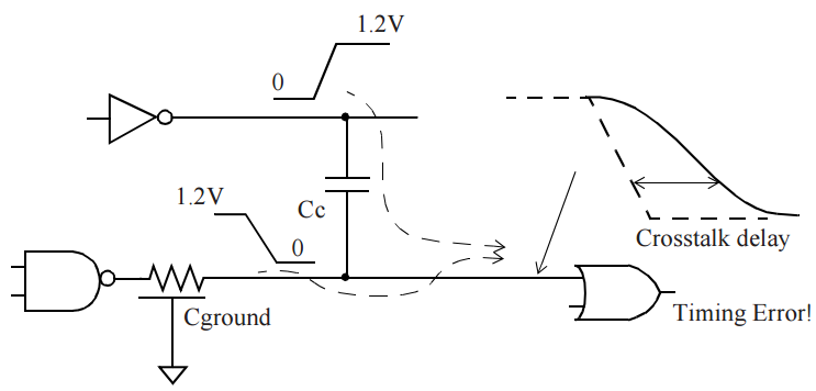 Figure 3 Positive crosstalk delay
The case of negative crosstalk delay is illustrated in Figure 4. The aggressor net is rising at the same time as the victim net. Aggressor net switching in the same direction as victim reduced delay of victim net. Negative crosstalk affects timing of driving cell as well as interconnect – delay for both of these is reduced.
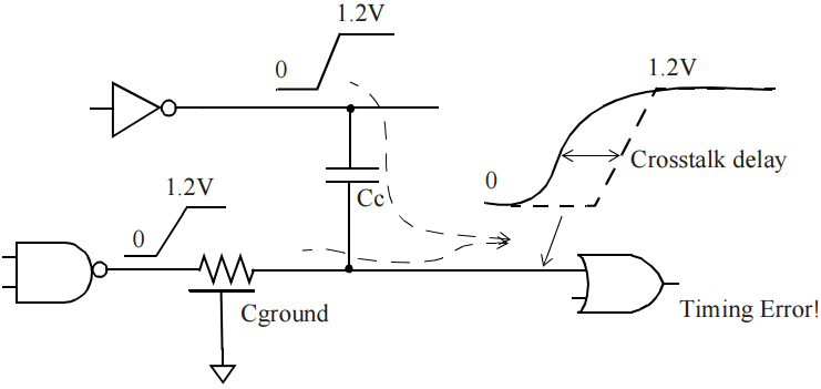 Figure 4 Negative crosstalk delay
Note that the worst positive and worst negative crosstalk delays are computed for rise and fall delays separately. The worst set of aggressor for rise max, rise min, fall max, fall min delay with crosstalk are different in general.
Comments
So empty here ... leave a comment!