Check clock gating

Figure 1 A clock gating check
A clock gating check occurs when a gating signal can control the path of a clock signal at a logic cell. An example is shown in Figure 1. The pin of logic cell connected to clock is called clock pin and pin where gating signal is connected to is gating pin. Logic cell where clock gating occurs is also referred to as gating cell.
One condition for a clock gating check is that clock that goes through cell must be used as a clock downstream. Downstream clock usage can be either as a FF clock or it can fanout to an output port or as generated clock that refers to output of gating cell as its master. If clock is not used as a clock after gating cell, then no clock gating check is inferred.
Another condition for clock gating check applies to gating signal. The signal at gating pin of check should not be a clock or if it was a clock, it should not be used as a clock downstream.
In a general scenario, clock signal and gating signal do not need to be connected to a single logic cell such as and, or or, but may be inputs to an arbitrary logic block. In such cases, for a clock gating check to be inferred, clock pin of the check must fan out to a common output pin.
There are two types of clock gating checks inferred:
- Active-high clock gating check: Occurs when gating cell has an and or a nand function.
- Active-low clock gating check: Occurs when gating cell has an or or a nor function.
Active-high and active-low refer to logic state of gating signal which activates clock signal at output of gating cell. If gating cell is a complex function where gating relationship is not obvious, such as a multiplexer or an xor cell, STA output will typically provide a warning that no clock gating check is being inferred. But this can be changed by specifying a clock gating relationship for gating cell explicitly by using command set_clock_gating_check. In such cases, if set_clock_gating_check specification disagrees with functionality of gating cell, STA will normally provide a warning.
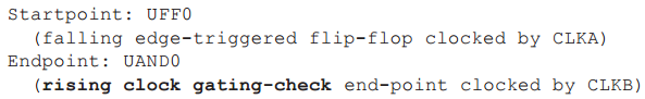
As specified earlier, a clock can be a gating signal only if it is not used as a clock downstream. Consider example in Figure 2. CLKB is not used as a clock downstream due to definition of generated clock of CLKA – path of CLKB is blocked by generated clock definition. Hence a clock gating check for clock CLKA is inferred for and cell.
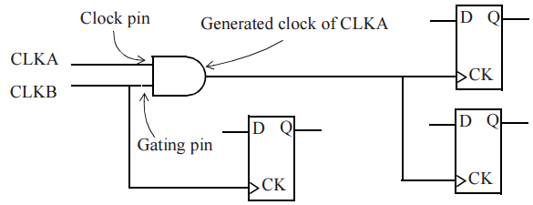
Figure 2 Gating check inferred – clock at gating pin not used as a clock downstream
Active-High Clock Gating
We examine timing relationship of an active-high clock gating check now. This occurs at an and or a nand cell; an example using and is shown in Figure 3. Pin B of gating cell is clock signal, and pin A of gating cell is gating signal.
Let us assume that both clocks CLKA and CLKB have the same waveform.
create_clock -name CLKA -period 10 \
-waveform {0 5} [get_ports CLKA]
create_clock -name CLKB -period 10 \
-waveform {0 5} [get_ports CLKB]
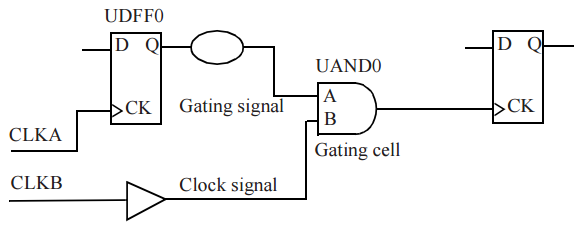
Figure 3 Active high clock gating using an AND cell
Because it is an and cell, a high on gating signal UAND0/A opens up gating cell and allows clock to propagate through. Clock gating check is intended to validate that gating pin transition does not create an active edge for fanout clock. For positive edge-triggered logic, this implies that rising edge of gating signal occurs during inactive period of clock (when it is low). Similarly, for negative edge-triggered logic, falling edge of gating signal should occur only when clock is low. Note that if clocks drives both positive and negative edge-triggered FF, any transition of gating signal (rising or falling edge) must occur only when clock is low. Figure 4 shows an example of a gating signal transition during active edge which needs to be delayed to pass clock gating check.

Figure 4 Gating signal needs to be delayed
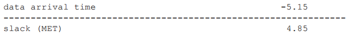
The active-high clock gating setup check requires that gating signal changes before clock goes high. Here is setup path report.

Notice that Endpoint indicates that it is a clock gating check. In addition, path is in clock_gating_default group of paths as specified in Path Group. Check validates that gating signal changes before next rising edge of clock CLKB at 10ns.
Active-high clock gating hold check requires that gating signal changes only after falling edge of clock. Here is hold path report.

Hold gating check fails because gating signal is changing too fast, before falling edge of CLKB at 5ns. If a 5ns delay was added between UDFF0/Q and UAND0/A1 pins, both setup and hold gating checks would pass validating that gating signal changes only in the specified window.
One can see that hold time requirement is quite large. This is caused by fact that sense of gating signal and FF being gated are the same. This can be resolved by using a different type of launch FF, a negative edge-triggered FF to generate gating signal.
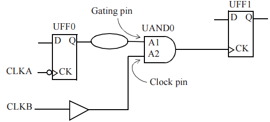
Figure 5 Gating signal clocked on falling edge
In Figure 5, FF UFF0 is controlled by negative edge of clock CLKA. Safe clock gating impies that the output of FF UFF0 must change during inactive part of gating clock, which is between 5ns and 10ns.
The signal waveform corresponding to schematic in Figure 5 are depicted in Figure 6. Here is clock gating setup report.

Figure 6 Gating signal generated from negative edge FF meets gating checks


Here is clock gating hold report. Notice that hold time check is much easier to meet with new design.
Since clock edge (negative edge) that launches gating signal is opposite of clock being gated (active-high), setup and hold requirements are easy to meet. This is the most common structure used for gated clocks.
Active-Low Clock Gating
Figure 7 shows an example of an active-low clock gating check.
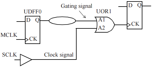
Figure 7 Active-low clock gating check
create_clock -name MCLK -period 8 \
-waveform {0 4} [get_ports MCLK]
create_clock -name SCLK -period 8 \
-waveform {0 4} [get_ports SCLK]
Active-low clock gating check validates that rising edge of gating signal arrives at active portion of clock (when it is high) for positive edge-triggered logic. As described previously, the key is that gating signal should not cause an active edge for output gated clock. When gating signal is high, clock cannot go through. Thus gating signal should switch only when clock is high as illustrated in Figure 8.
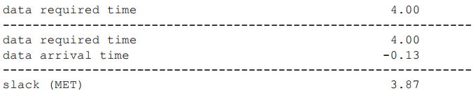
Here is active-low clock gating setup timing report. This check ensures that gating signal arrives before clock edge becomes inactive, in this case, at 4ns.

Figure 8 Gating signal changes when clock is high

Here is clock gating hold timing report. This check ensures that gating signal changes only after rising edge of clock signal, which in this case is at 0ns.

Clock Gating with a Multiplexer
Figure 9 shows an example of clock gating using a multiplexer cell. A clock gating check at multiplexer inputs ensures that multiplexer select signal arrives at right time to clearly switch between MCLK and TCLK. For example, we are interested in switching to and from MCLK and assume that TCLK is low when select signal switches. This implies that select signal of multiplexer should switch only when MCLK is low. This similar to active-high clock gating check.
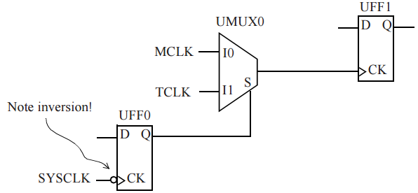
Figure 9 Clock gating using a multiplexer

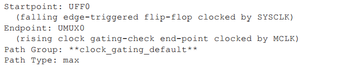
Figure 10 Gating signal arrives when clock is low
Figure 10 shows timing relationships. The select signal for multiplexer must arrive at time MCLK is low. Also, assume TCLK will be low when select changes.
Since gating cell is a multiplexer, clock gating check is not inferred automatically, as evidenced in this message reported during STA.
Warning: No clock-gating check is inferred for clock MCLK at pins UMUX0/S and UMUX0/I0 of cell UMUX0. Warning: No clock-gating check is inferred for clock TCLK at pins UMUX0/S and UMUX0/I1 of cell UMUX0.
But a clock gating check can be explicitly forced by providing a set_clock_gating_check specification.
set_clock_gating_check -high \
[get_cells UMUX0]
# The -high option indicates an active-high check.
set_disable_clock_gating_check UMUX0/I1
The disable check turns off clock gating check on specific pin, as we are not concerned with this pin. Clock gating check on multiplexer has been specified to be an active-high clock gating check.

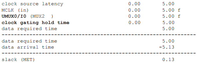
Here is setup timing path report.

The clock gating hold timing report is next.

Comments
So empty here ... leave a comment!