Sequential cells timing models
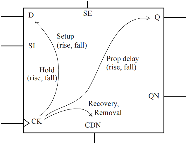
Figure 1 Sequential cell timing arcs
Consider timing arcs of a sequential cell shown in Figure 1. For synchronous inputs, such as D pin (or SI, SE), there are following timing arcs:
i. Setup check arc (rising and falling)
ii. Hold check arc (rising and falling)
For asynchronous inputs, such as CDN pin, there are following timing arcs:
i. Recovery check arc
ii. Removal check arc
For synchronous output of a FF, such as Q or QN pins, there is following timing arc:
i. CK-to-output propagation delay arc (rising and falling)
All of synchronous timing arcs are with respect to active edge of clock, edge of clock that causes sequential cell to capture data. In addition, clock pin and asynchronous pins such as clear, can have pulse width timing checks.
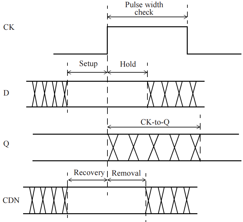 Figure 2 Timing arcs on an active rising clock edge
Figure 2 shows timing checks using various signal waveforms.
1. Synchronous checks: Setup and Hold
Setup and hold synchronous timing checks are needed for proper propagation of data through sequential cells. These checks verify that data input is unambiguous at active edge of clock and proper data is latched in at active edge. These timing checks validate if data input is stable around active clock edge. The minimum time before active clock when data input must remain stable is called setup time. This is measured as time interval from the latest data signal crossing its threshold (normally 50% of Vdd) to active clock edge crossing its threshold (normally 50% of Vdd).
Similarly, hold time is the minimum time data input must remain stable just after active edge of clock. This is measured as time interval from active clock edge crossing it threshold to earliest data signal crossing it threshold. As mentioned previously, active edge of clock for a sequential cell is rising and falling edge that causes sequential cell to capture data.
Example of Setup and Hold checks
Setup and hold constraints for a synchronous pin of a sequential cell are normally described in terms of 2D tables as illustrated below.
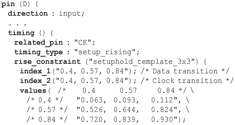
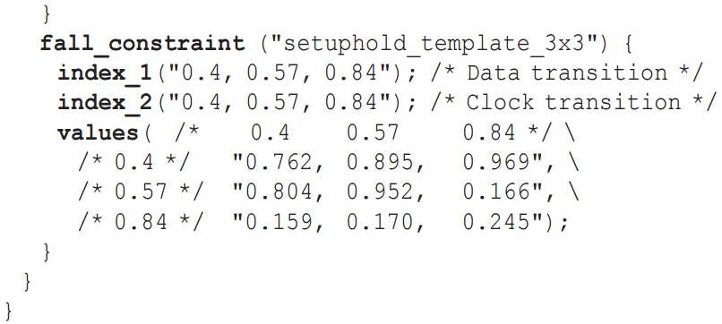
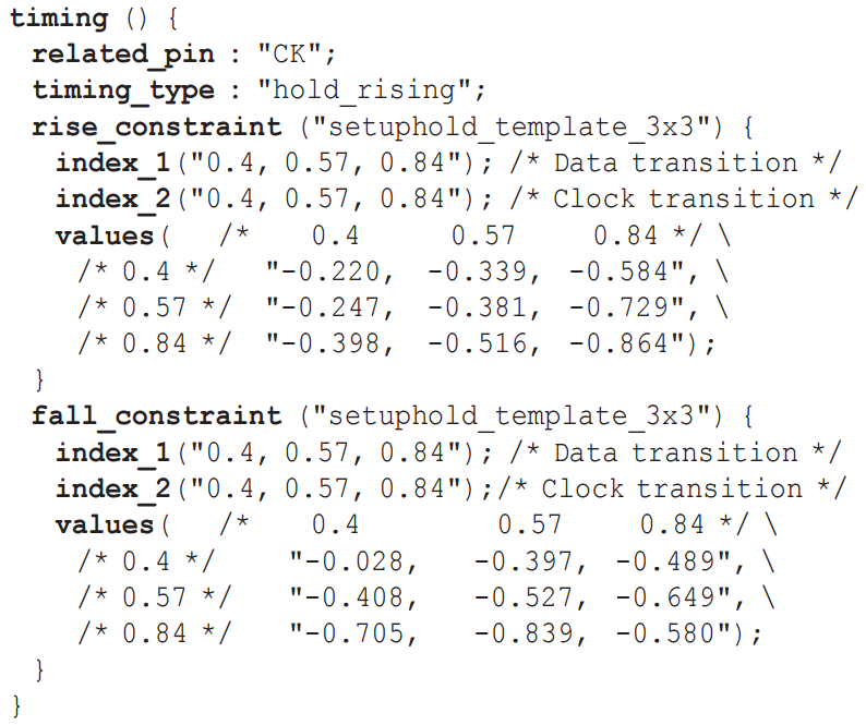
Example above shows setup and hold constraints on input D pin with respect to rising edge of clock CK of a sequential cell. 2D models are in terms of transition times at constraint pin (D) and related pin (CK).
Negative values in setup and hold checks
Notice that some of hold values in example above are negative. This is acceptable and normally happens when path from pin of FF to internal latch point for data is longer than corresponding path for clock. Thus, a negative hold check implies that data pin of FF can change ahead of clock pin and still meet hold time check.
Setup values of a FF can also be negative. This means that pins of FF, data can change after clock pin and still meet setup time check.
Can both setup and hold be negative? No. For setup and hold checks to be consistent, sum of setup and hold values should be positive. Thus, if setup (or hold) check contains negative values – corresponding hold (or setup) should be sufficiently positive so that setup plus hold value is a positive quantity.
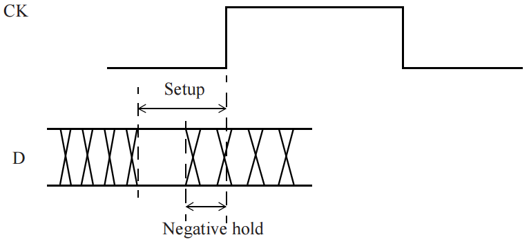 Figure 3 Negative value for hold timing check
For FF, it is helpful to have a negative hold time on scan data input pins. This gives flexibility in terms of clock skew and can eliminate need for almost all buffer insertion for fixing hold violations in scan mode (scan mode is the one in which FFs are tied serially forming a scan chain – output of FF is typically connected to scan data input pin of the next FF in series; these connections are for test-ability).
Similar to setup or hold check on synchronous data inputs, there are constraint checks governing asynchronous pins.
2. Asynchronous checks
Recovery and Removal checks
Asynchronous pins such as asynchronous clear or asynchronous set override any synchronous behavior of cell. When an asynchronous pin is active, output is governed by asynchronous pin and not by clock latching in data inputs. However, when asynchronous pin becomes inactive, active edge of clock starts latching in data input. Asynchronous recovery and removal constraint checks verify that asynchronous pin has returned unambiguously to an inactive state at next active clock edge.
Recovery time is the minimum time that an asynchronous input is stable after being de-asserted before next active clock edge.
Similarly, removal time is the minimum time after an active clock edge that asynchronous pin must remain active before it can be de-asserted.
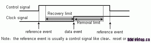
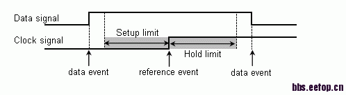
Figure 4 Recovery (Removal) vs Setup (Hold)
Pulse width checks
In addition to synchronous and asynchronous timing checks, there is a check which ensures that pulse width at an input pin of a cell meets minimum requirement. For example, if width of pulse at clock pin is smaller than specified minimum, clock may not latch data properly. The pulse width checks can be specified for relevant synchronous and asynchronous pins also. The minimum pulse width checks can be specified for high pulse and for low pulse also.
Example of Recovery, Removal and Pulse width checks
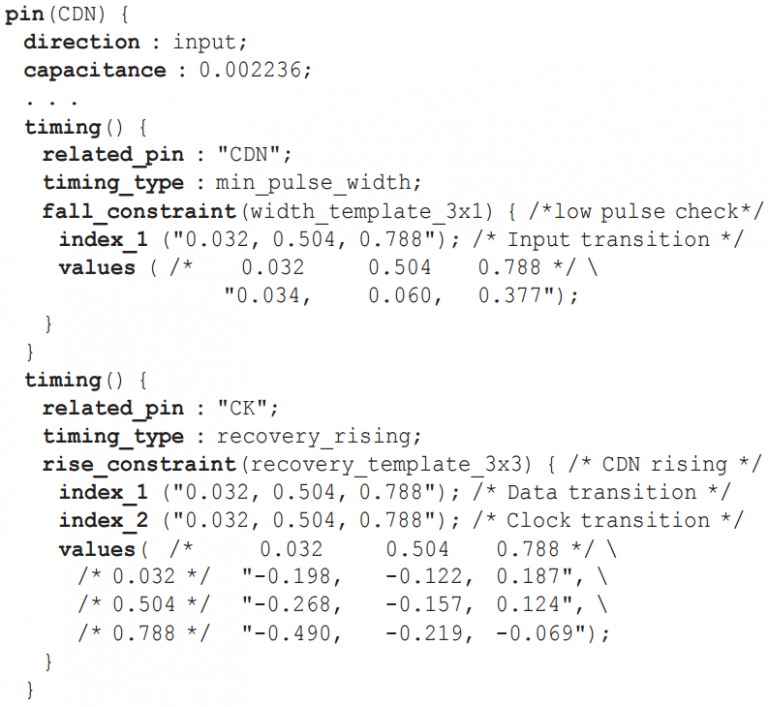

An example of recovery time, removal time, (both of them are with respect to clock pin CK) and pulse width check for an asynchronous clear pin CDN of a FF is given above.
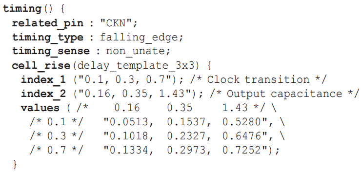
3. Propagation delay
Propagation delay of a sequential cell is from active edge of clock to a rising or falling edge on output. This is a non-unate timing arc as the active edge of clock can cause either a rising or a falling edge on ouput Q. Here is an example of a propagation delay arc for a negative edge-triggered FF, from clock pin CKN to output Q.


Comments
So empty here ... leave a comment!