Cadence Virtuoso
Design an Electromigration (EM) Test Pad
University of Central Florida
Designed an Electromigration (EM) Test Pad layout using Cadence® Virtuoso® for tape-out in collaboration with Harris Corporation and ICAMR (Fall 2016); submitted GDSII files to partner Novati Technologies, Inc.
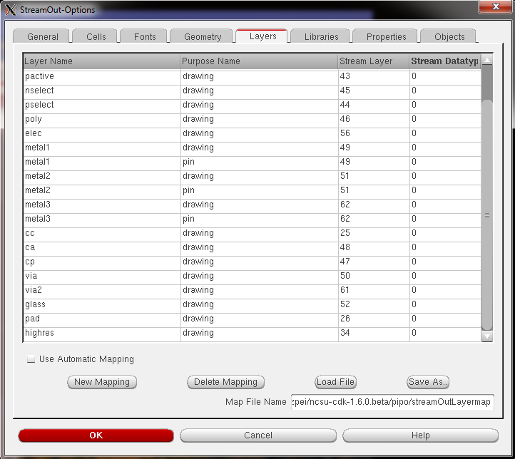
Map file was from MOSIS: https://www.eda.ncsu.edu/wiki/MOSIS_Layers, https://eda.ncsu.edu/.
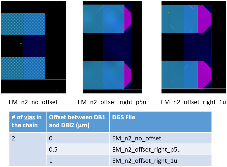
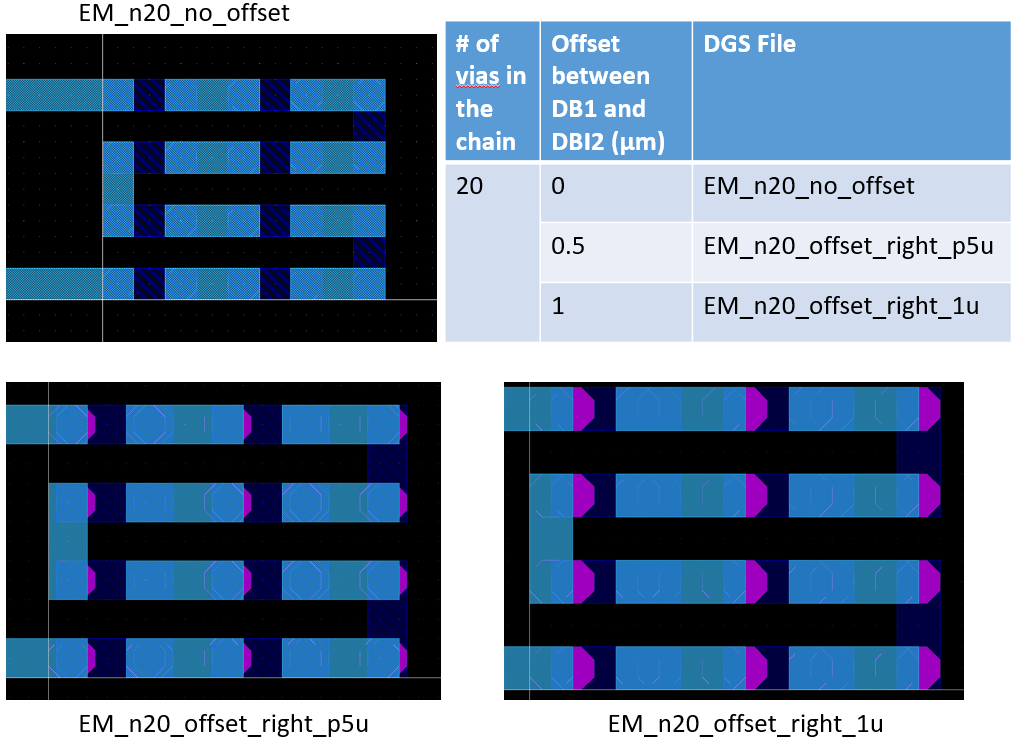
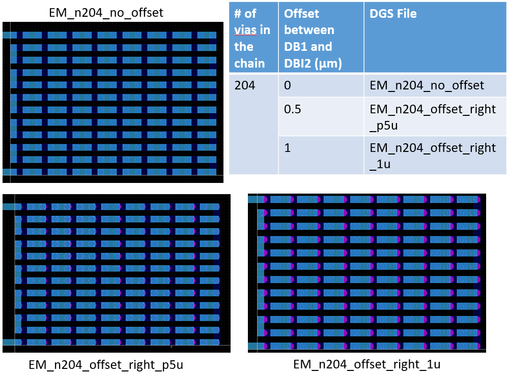
The test pad size: 120um x 120 um. Pitch: 250um, which means 130um spacing between 2 test pads, with maligned vias, or different numbers of links, or different trace widths.
The stack-up was M1, DBI1, DBI2, M2. DBI1 and DBI2 are nominally identical, unless the designer wanted to intentionally misalign them.
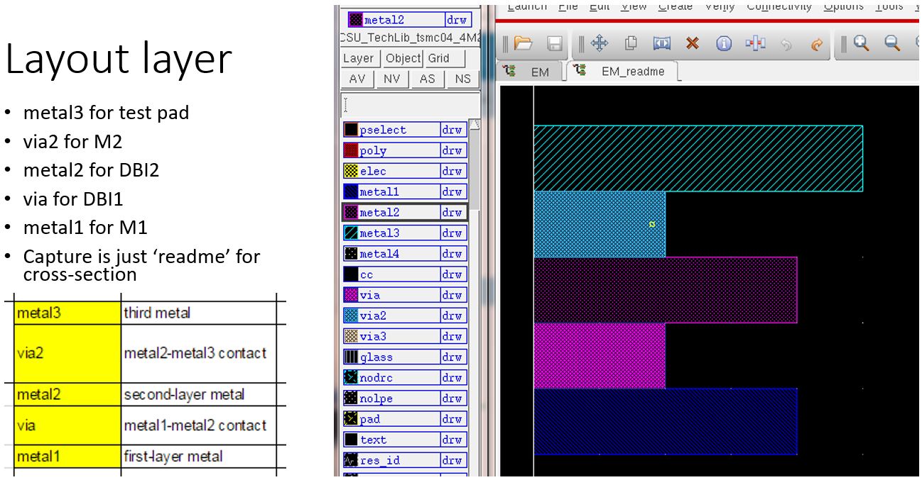
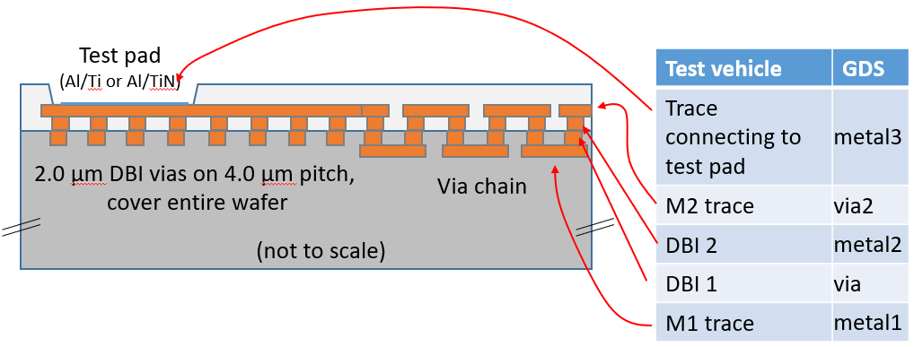
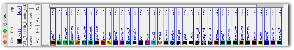
Virtuoso layout layers: metal 1 was the first-layer metal, via was metal1-metal2 contact, metal 2 was the second-layer metal, via2 was the metal2-metal3 contact, metal3 was the third metal. For EM Test Pad foundry, metal1 was for M1, via was for DBI1, metal2 was for DBI2, via 2 was for M2, and metal3 was for test pad.
Cadence Products Run on a variety of UNIX- and PC-based Systems
Remote access to the Linux Servers
Macintosh User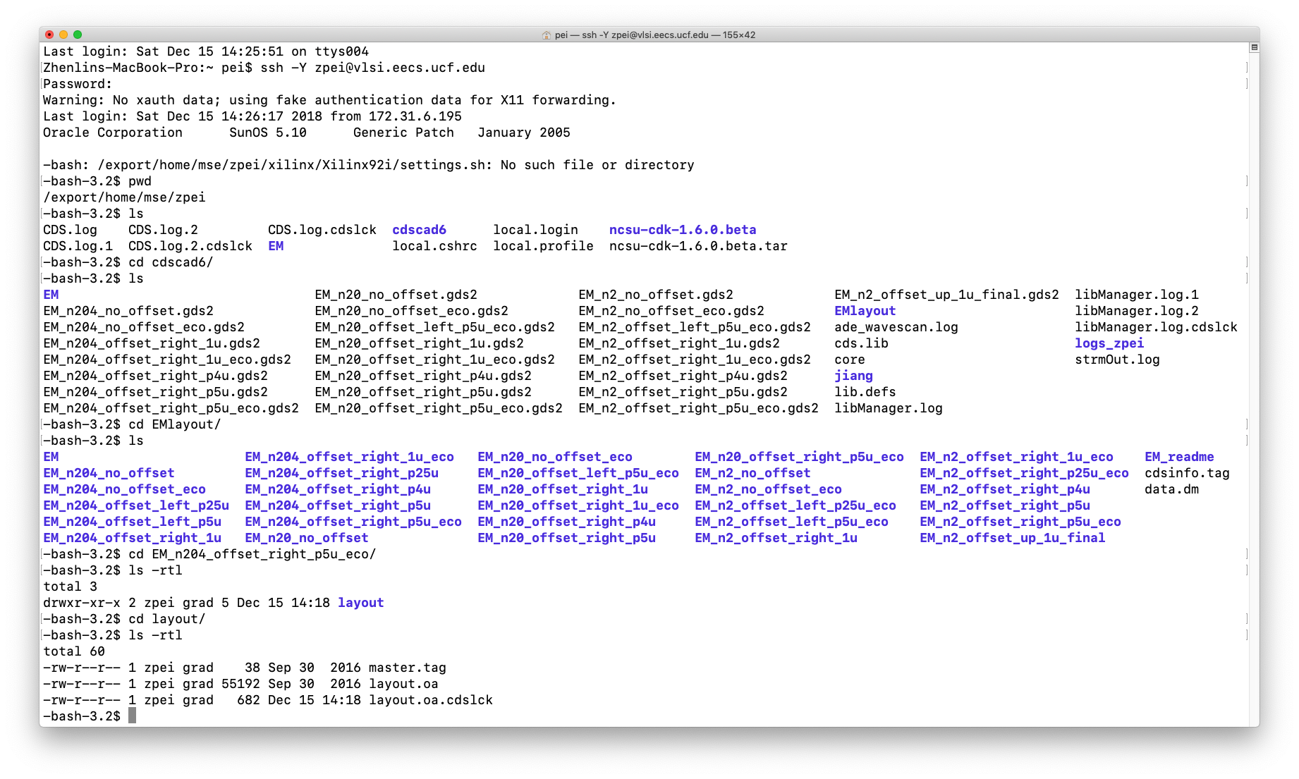
Running Cadence Virtuoso®
icfb
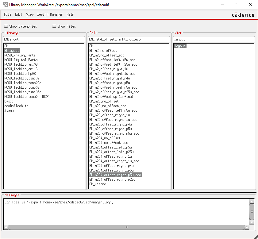
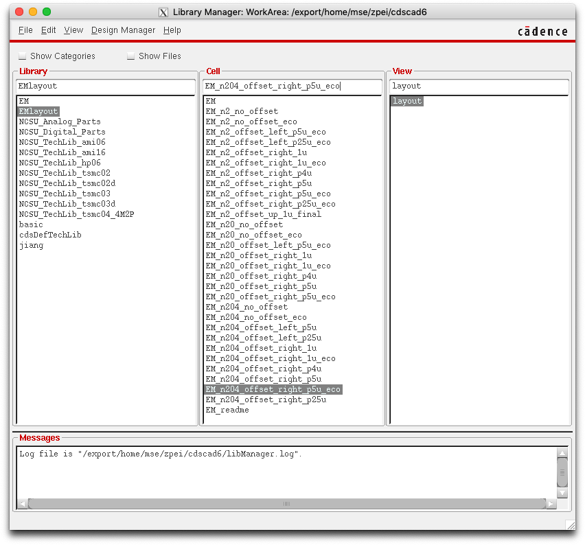
Library Manager
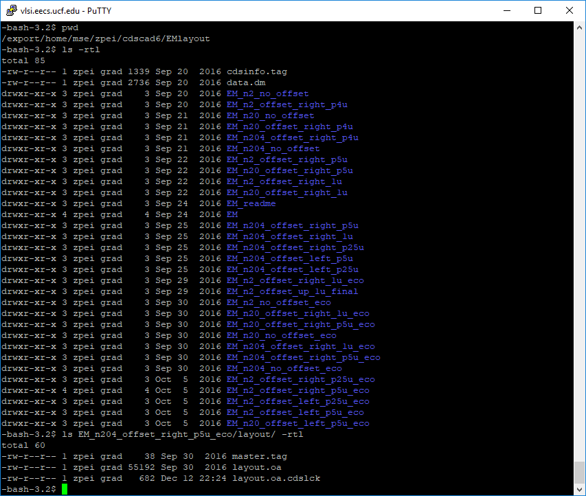
WorkArea: /export/home/mse/zpei/cdscad6
-bash-3.2$ pwd
/export/home/mse/zpei/cdscad6/EMlayout
-bash-3.2$ ls -rtl
total 85
-rw-r–r– 1 zpei grad 1339 Sep 20 2016 cdsinfo.tag
-rw-r–r– 1 zpei grad 2736 Sep 20 2016 data.dm
drwxr-xr-x 3 zpei grad 3 Sep 20 2016 EM_n2_no_offset
drwxr-xr-x 3 zpei grad 3 Sep 20 2016 EM_n2_offset_right_p4u
drwxr-xr-x 3 zpei grad 3 Sep 21 2016 EM_n20_no_offset
drwxr-xr-x 3 zpei grad 3 Sep 21 2016 EM_n20_offset_right_p4u
drwxr-xr-x 3 zpei grad 3 Sep 21 2016 EM_n204_offset_right_p4u
drwxr-xr-x 3 zpei grad 3 Sep 21 2016 EM_n204_no_offset
drwxr-xr-x 3 zpei grad 3 Sep 22 2016 EM_n2_offset_right_p5u
drwxr-xr-x 3 zpei grad 3 Sep 22 2016 EM_n20_offset_right_p5u
drwxr-xr-x 3 zpei grad 3 Sep 22 2016 EM_n2_offset_right_1u
drwxr-xr-x 3 zpei grad 3 Sep 22 2016 EM_n20_offset_right_1u
drwxr-xr-x 3 zpei grad 3 Sep 24 2016 EM_readme
drwxr-xr-x 4 zpei grad 4 Sep 24 2016 EM
drwxr-xr-x 3 zpei grad 3 Sep 25 2016 EM_n204_offset_right_p5u
drwxr-xr-x 3 zpei grad 3 Sep 25 2016 EM_n204_offset_right_1u
drwxr-xr-x 3 zpei grad 3 Sep 25 2016 EM_n204_offset_right_p25u
drwxr-xr-x 3 zpei grad 3 Sep 25 2016 EM_n204_offset_left_p5u
drwxr-xr-x 3 zpei grad 3 Sep 25 2016 EM_n204_offset_left_p25u
drwxr-xr-x 3 zpei grad 3 Sep 29 2016 EM_n2_offset_right_1u_eco
drwxr-xr-x 3 zpei grad 3 Sep 29 2016 EM_n2_offset_up_1u_final
drwxr-xr-x 3 zpei grad 3 Sep 30 2016 EM_n2_no_offset_eco
drwxr-xr-x 3 zpei grad 3 Sep 30 2016 EM_n20_offset_right_1u_eco
drwxr-xr-x 3 zpei grad 3 Sep 30 2016 EM_n20_offset_right_p5u_eco
drwxr-xr-x 3 zpei grad 3 Sep 30 2016 EM_n20_no_offset_eco
drwxr-xr-x 3 zpei grad 3 Sep 30 2016 EM_n204_offset_right_1u_eco
drwxr-xr-x 3 zpei grad 3 Sep 30 2016 EM_n204_offset_right_p5u_eco
drwxr-xr-x 3 zpei grad 3 Sep 30 2016 EM_n204_no_offset_eco
drwxr-xr-x 3 zpei grad 3 Oct 5 2016 EM_n2_offset_right_p25u_eco
drwxr-xr-x 4 zpei grad 4 Oct 5 2016 EM_n2_offset_right_p5u_eco
drwxr-xr-x 3 zpei grad 3 Oct 5 2016 EM_n2_offset_left_p25u_eco
drwxr-xr-x 3 zpei grad 3 Oct 5 2016 EM_n2_offset_left_p5u_eco
drwxr-xr-x 3 zpei grad 3 Oct 5 2016 EM_n20_offset_left_p5u_eco
-bash-3.2$ ls EM_n204_offset_right_p5u_eco/layout/ -rtl
total 60
-rw-r–r– 1 zpei grad 38 Sep 30 2016 master.tag
-rw-r–r– 1 zpei grad 55192 Sep 30 2016 layout.oa
-rw-r–r– 1 zpei grad 682 Dec 12 22:24 layout.oa.cdslck
-bash-3.2$
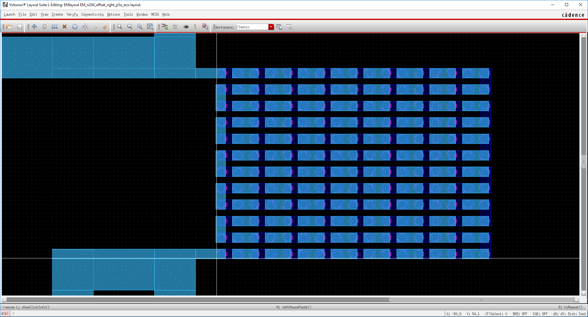
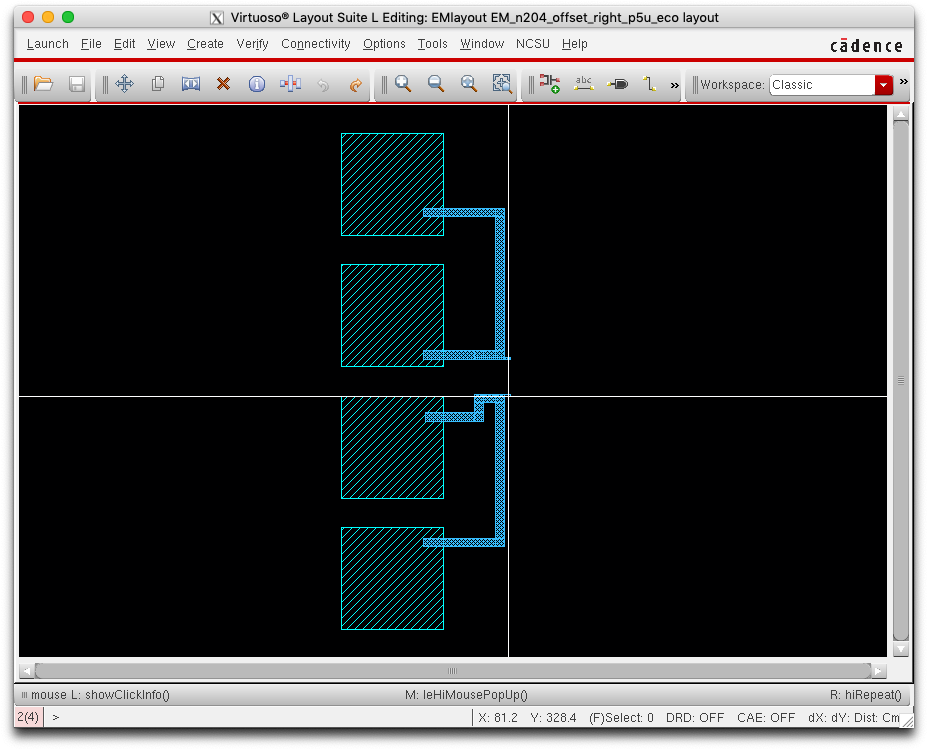
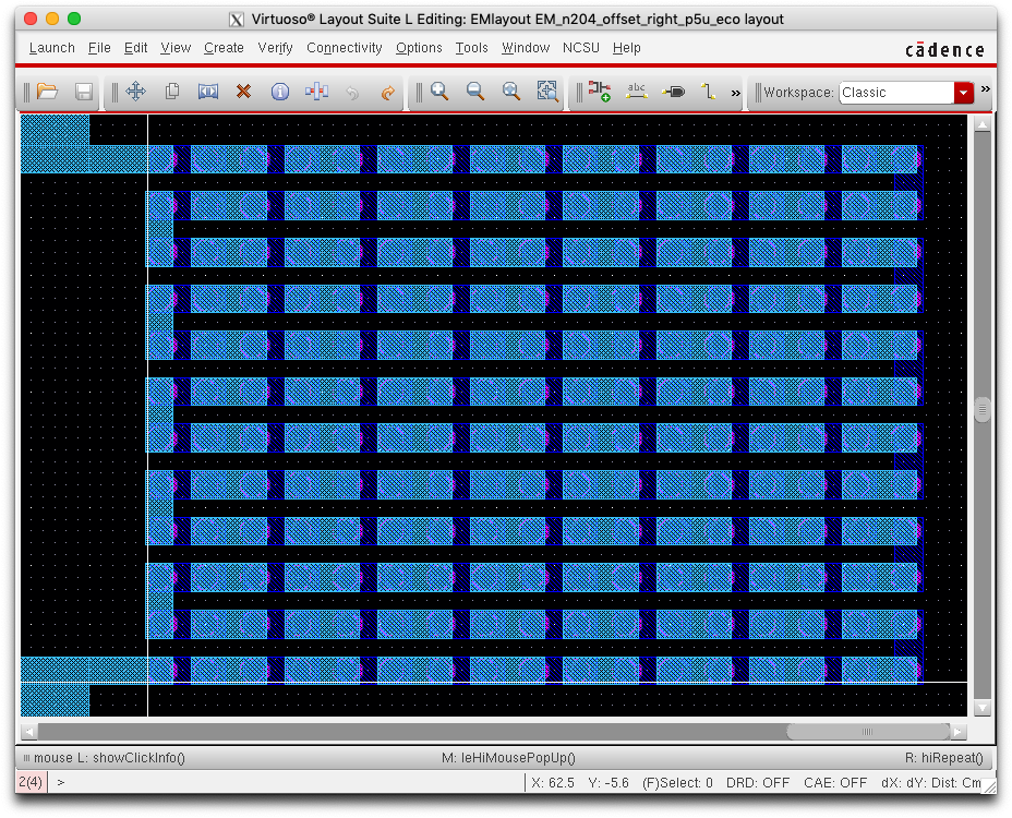
Layout for Electromigration Test Pad
Virtuoso® Layout Suite L Editing: EMlayout EM_n204_offset_right_p5u_eco
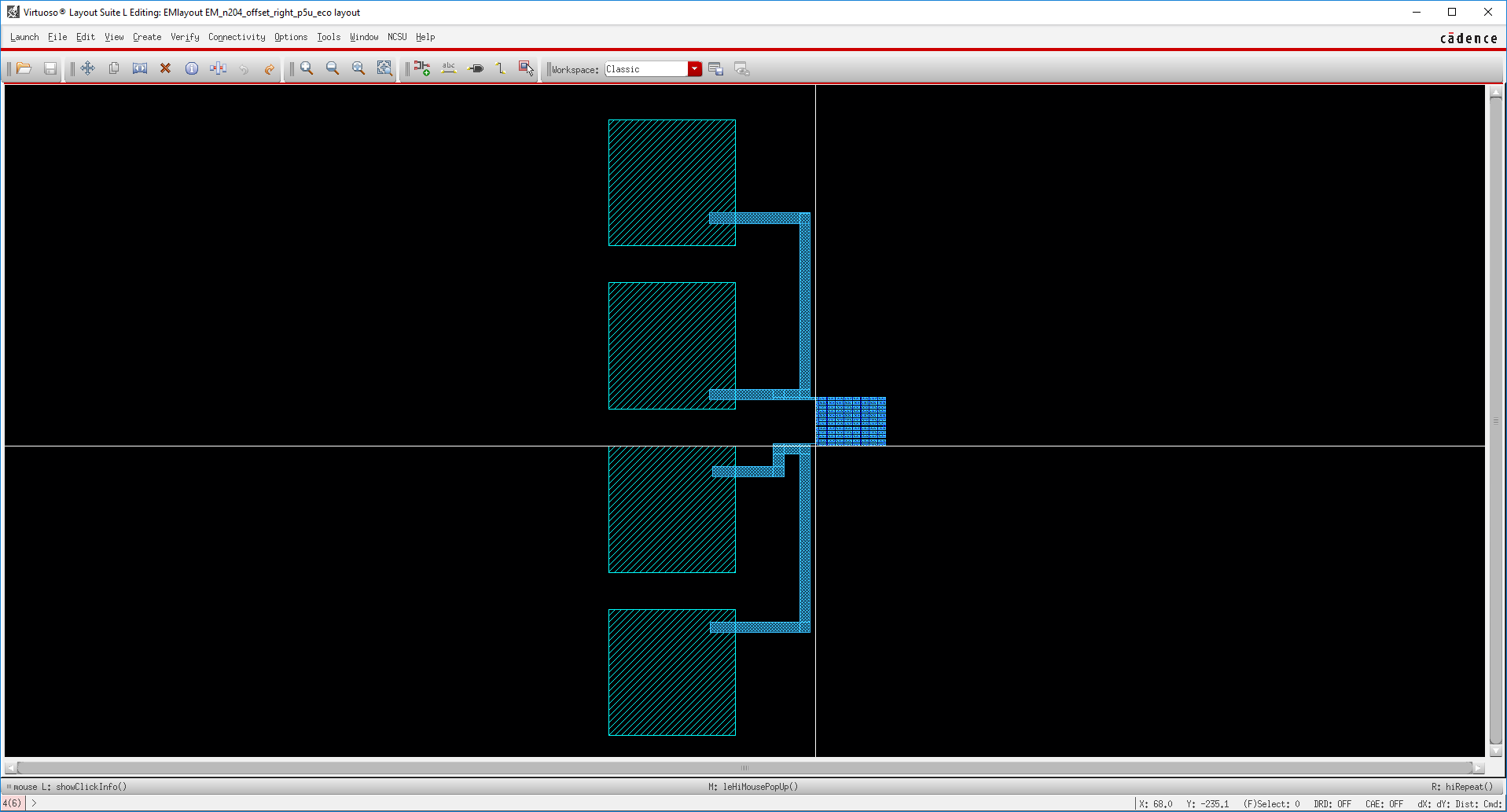
Zoom in to review the 204-via in chain geometry

Layout MOSIS IC Layer Information
https://www.eda.ncsu.edu/wiki/MOSIS_Layers
Test pad size: 120um x 120 um. Pitch: 250um, which means 130um spacing between 2 test pads. 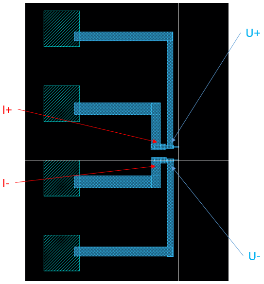 With maligned vias, or different numbers of links, or different trace widths. Make the layouts for offset (+x positive is right). Submitted GDSII to Novati Technologies, Inc. For Harris Corporation and ICAMR.
- Bottom wafer layers are M1 and DB1; top wafer (thinned) are M2 and DB2.
- DBI1/DBI2 thicknesses is 1.5 um. M1/M2 thicknesses is 1 um.
- DBI is about 3.14/16 ~ 20%. M1 and M2 is ~2.4/4 = 60% on interior of via chains and combs.
- Here is how the layers in GDS files corresponding to layers in the test vehicle.
Summary of EM Structures
Macintosh User
Comments
So empty here ... leave a comment!