PN junction
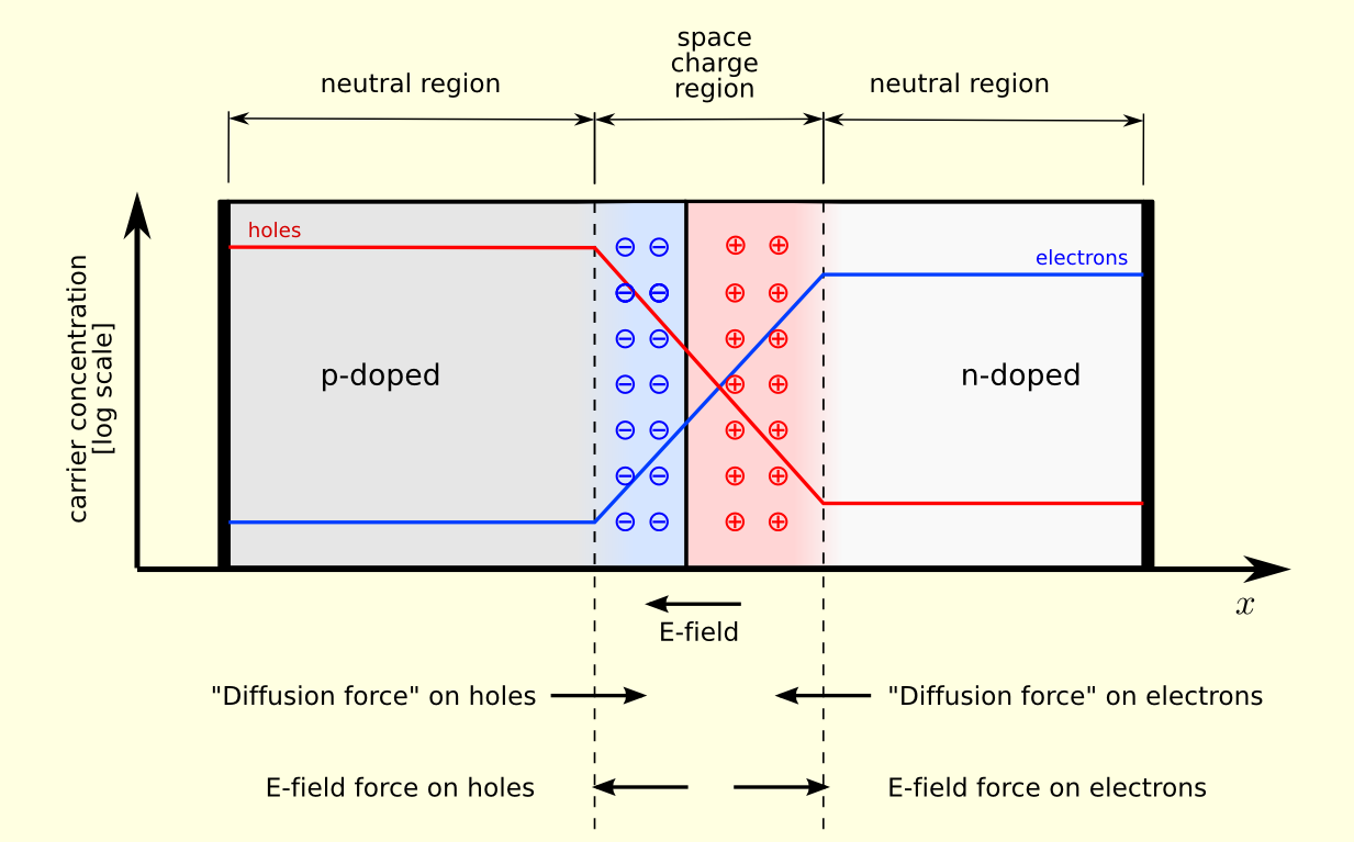
Figure A. A p–n junction in thermal equilibrium with zero-bias voltage applied. Electron and hole concentration are reported with blue and red lines, respectively. Gray regions are charge-neutral. Light-red zone is positively charged. Light-blue zone is negatively charged. The electric field is shown on the bottom, the electrostatic force on electrons and holes and the direction in which the diffusion tends to move electrons and holes.
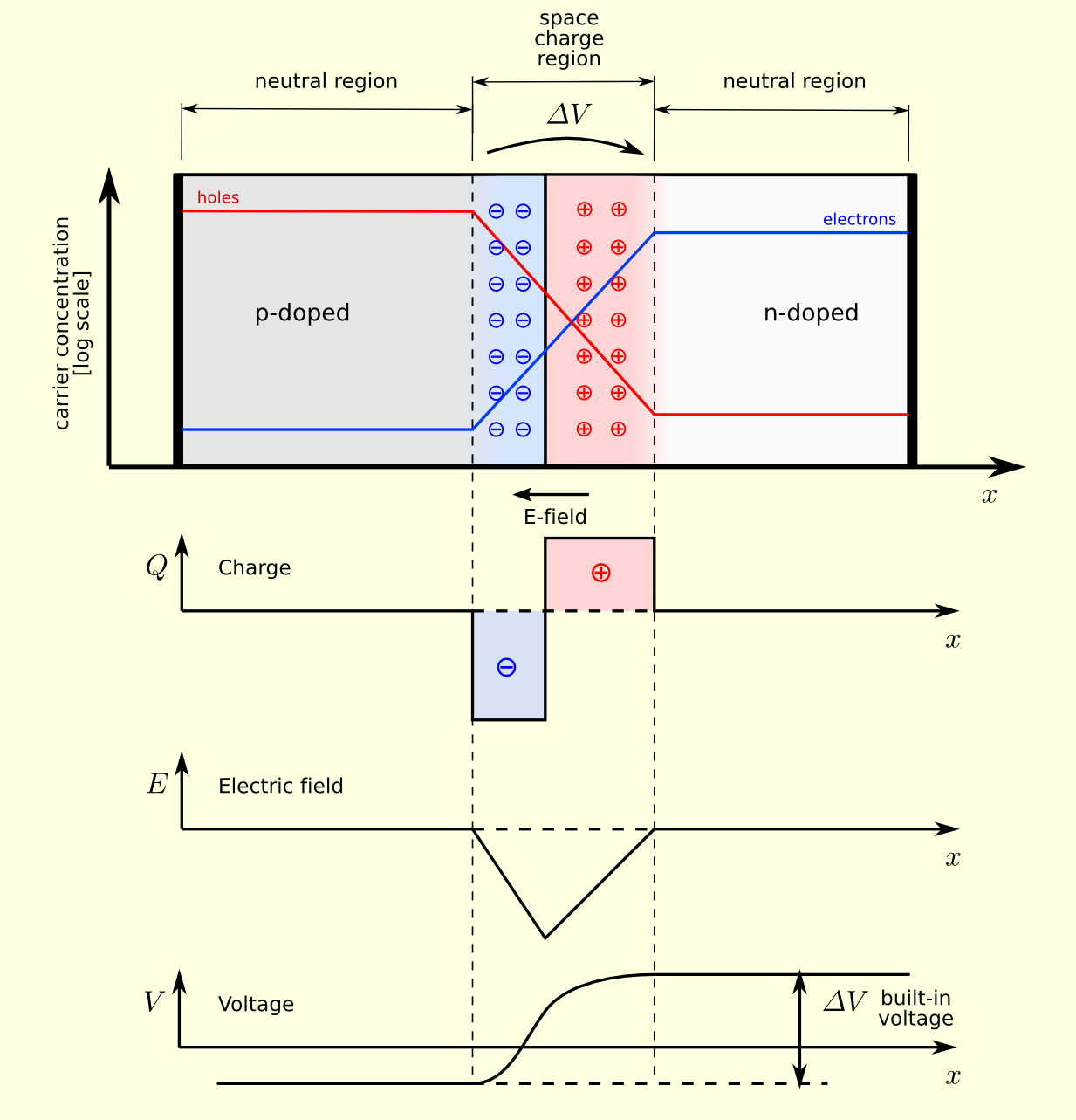
Figure B. A p–n junction in thermal equilibrium with zero-bias voltage applied. Under the junction, plots for the charge density, the electric field, and the voltage are reported.
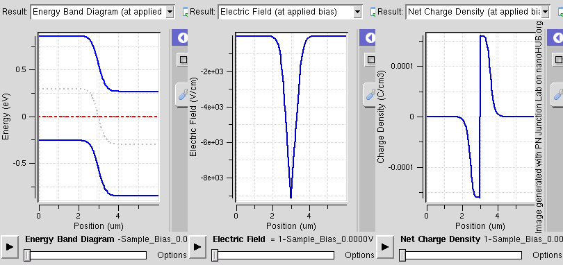
PN junction operation in forward-bias mode, showing reducing depletion width. Both p and n junctions are doped at a 1e15/cm3 doping level, leading to built-in potential of ~0.59 V. Reducing depletion width can be inferred from the shrinking charge profile, as fewer dopants are exposed with increasing forward bias.
 A silicon p–n junction in reverse bias.
Summary
The forward-bias and the reverse-bias properties of the p–n junction imply that it can be used as a diode. A p–n junction diode allows electric charges to flow in one direction, but not in the opposite direction; negative charges (electrons) can easily flow through the junction from n to p but not from p to n, and the reverse is true for holes. When the p–n junction is forward-biased, electric charge flows freely due to reduced resistance of the p–n junction. When the p–n junction is reverse-biased, however, the junction barrier (and therefore resistance) becomes greater and charge flow is minimal.
-from https://en.wikipedia.org/wiki/P%E2%80%93n_junction
Comments
So empty here ... leave a comment!