 Columbia Integrated Systems Laboratory, Columbia University
Design a broad-band amplifier
- Course: Analog Electronic Circuits (Prof. Yannis Tsividis), Fall 2009
- Designed the circuit under the guidance of Professor Yannis P. Tsividis and submitted a comprehensive summary of the design project.
- Fabricated and validated circuits using the breadboard.
- Used PSPICE to develop a broad-band amplifier which meet voltage gain: more than 60 dB, pass-band: from ≤100 Hz to ≥100 kHz, frequency response variation: less than 3 dB within pass-band, total harmonic distortion with 4 V peak-to-peak output: < 1 % @ 1 KHz. Under operation environment: temperature range: 0 ~ 85 °C, supply voltage: 9 V ± 0.5 V (single), source resistance: 50 Ω, load resistance: 1 KΩ. Let supply current: as low as possible, used only a single power supply, resistors, capacitors, and 2N2222A transistors.
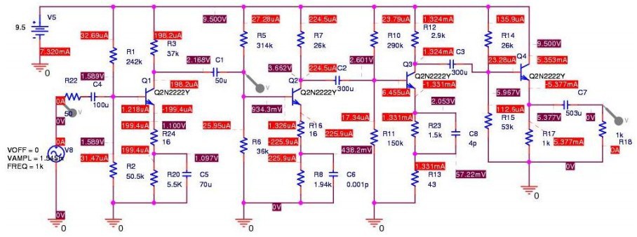 Fig. 1 Schematic of Circuit
The parameter values of the circuit components are listed in Table 1.
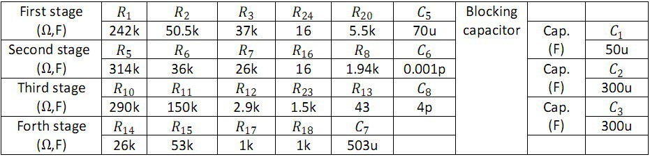 Table 1 Circuit Design
Results
The Q-point and supply voltage/current values are listed in Table 2.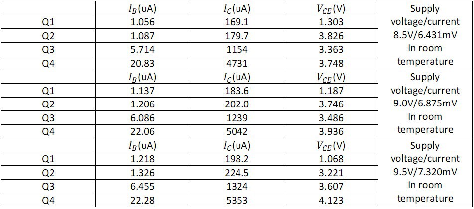
Table 2 Value of Q-point and Supply Voltage/Current
Fig. 2 shows the voltage gain at temperatures of 0, 5, 15, 25, 35, 45, 55, 65, 75, and 85 °C with an 8.5 V supply voltage.
 Fig. 2 Voltage Gain for Supply Voltage of 8.5V
Fig. 3 shows the voltage gain at temperatures of 0, 5, 15, 25, 35, 45, 55, 65, 75, and 85 °C with an 9.0 V supply voltage.
 Fig. 3 Voltage Gain for Supply Voltage of 9.0V
Fig. 4 shows the voltage gain at temperatures of 0, 5, 15, 25, 35, 45, 55, 65, 75, and 85 °C with an 9.5 V supply voltage.
 Fig. 4 Voltage Gain for Supply Voltage of 9.5V
Table 3 presents the THD* (Total Harmonic Distortion) values for a 4 VP-P output at 1 KHz across different temperatures, indicating the worst-case output performance.
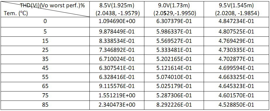 Table 3 THD and Worst-case Output Performance