Researchers design an accessible, straightforward technique to characterize moiré systems – a class of materials built by placing slightly misaligned atomic monolayers on top of each other. Under certain conditions, such moiré structures exhibit exotic physical phenomena absent in the individual units that conform them.
A moiré pattern is an interference effect that arises when two grids are superimposed. It can be observed in the wrinkles of a mesh shirt and it is responsible for the fringes that appear when taking a picture of a computer screen. Moiré patterns are present in art and fashion, and in the last few years their effect in two-dimensional materials has entailed a revolution in physics.
Two-dimensional materials are those that are less than a nanometer thick. The first one to be isolated was graphene, a single-layer of carbon atoms (see Fig. 1a). Such discovery opened a whole new field of research and many labs around the world started making their own stacks – structures with two-dimensional materials placed on top of each other. If one were to place one of those layers slightly misaligned with the one below, a moiré pattern would emerge. This interference effect can be visualized in Fig. 1b. The small circles represent the carbon atoms that form a crystalline lattice (an ordered structure) on each graphene layer. The top layer is rotated with respect to the bottom one and, as a consequence, a periodicity larger than the atomic lattice emerges as highlighted in Fig. 1b.
In 2018, the field of condensed matter physics was stirred up: such moiré materials, at a very specific misalignment value called the magic angle, exhibit electronic states of matter that are not present in the individual layers, such as superconductivity or magnetism. The emergence of those electronic phases is a consequence of the moiré pattern and its direct visualization is critical for their understanding. There are a few techniques, including transmission electron microscopy and scanning tunneling microscopy that allow for this, but they require complex setups that do not necessarily work for any material, which has significantly slowed down the progress in the field. McGilly and colleagues show a new and simple technique based on piezoresponse force microscopy to visualize moiré patterns.
A piezoresponse force microscope consists of a sharp metallic tip brought into contact with the material under study – in this case, the moiré system (see Fig. 1c). Piezoresponsive materials are those that undergo a mechanical deformation in the presence of an electric field. In the microscope, the sample moves a small amount when a voltage is applied across it and the tip follows the motion. Such tip motion is measured as a voltage which is amplified to detectable values. The tip is then moved around the sample and the process is repeated on every pixel of a selected region, producing a map of the sample’s deformation.
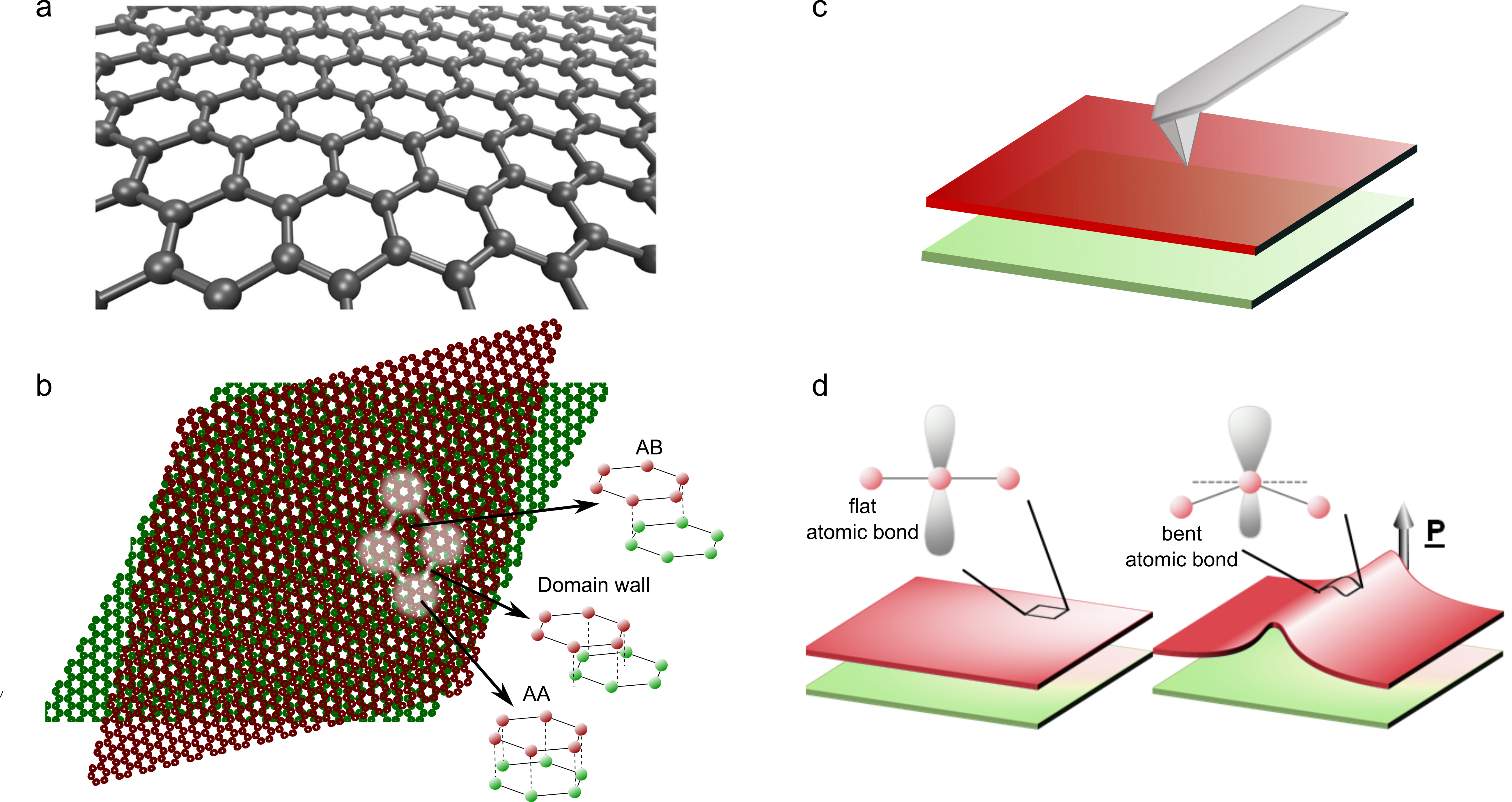
In principle, it was not obvious that a moiré pattern would be detectable with the microscope. When moiré patterns form, it creates a repetitive set of individual units that are called unit cells (highlighted region in Fig. 1b). Each unit cell is formed by regions with different atomic three-dimensional configurations, called sites. In the case of graphene, those sites are called AA and AB which stands for how the atoms from each layer lie on top of each other (see insets in Fig. 1b). The AB regions (also called domains) are separated by domain walls, as highlighted in Fig. 1b. McGilly and colleagues show that the voltage signal detected with the microscope is localized on the domain walls.
When the moiré pattern forms, the atomic layers relax to accommodate it and the layer wrinkles along the domain wall (see right panel in Fig. 1d). Since the microscope is not sensitive to such small deformation, the origin of the detected signal must be electronic. Flat graphene layers have planar bonds, as shown in the left panel of Fig. 1d. However, the curvature of the wrinkle bends the atomic bonds on the graphene layer, which in turn causes an asymmetric distribution of the charge in the vertical direction and gives rise to an out-of-plane polarization (P), which is responsible for the signal measured in the microscope.
The technique designed by McGilly and colleagues has been proven extremely useful for the advancement of the field due to the simplicity of the method and the fact that it allows imaging of any moiré pattern, independently of the nature of the individual units that conform it – that is, whether they are metals, semiconductors or insulators. Being able to image moiré patterns with such an accessible technique will help improve the fabrication process, and having uniform samples is critical since strain gradients can significantly alter the states of matter that emerge in moiré materials.
Dr. Leo McGilly is a Postdoctoral Research Fellow in the Physics Department at Columbia University.